Introduction
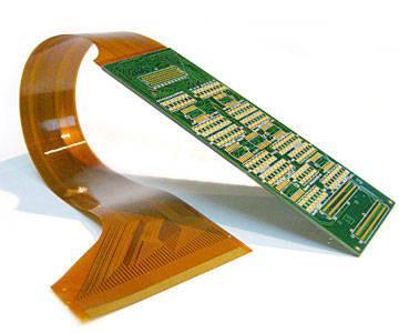
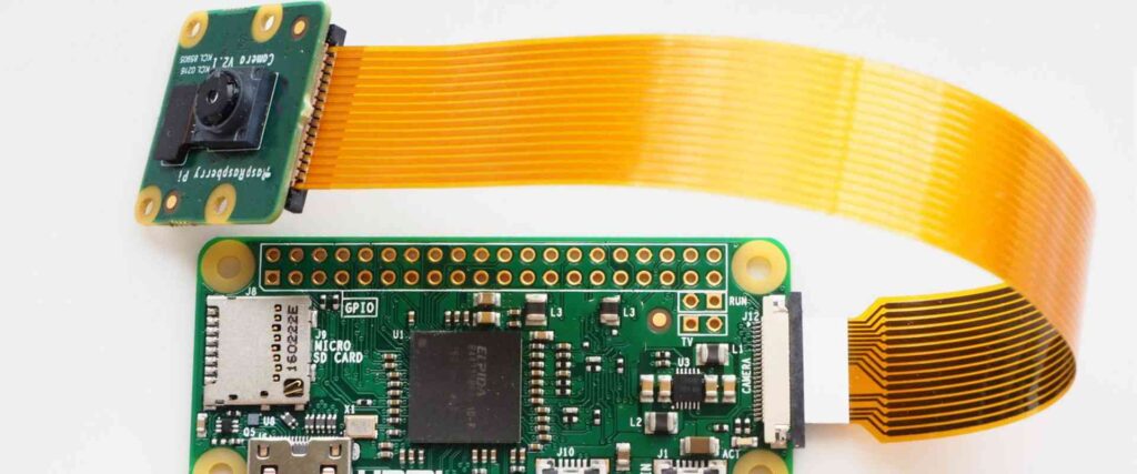
A rigid flexible printed circuit board (rigid flex PCB) combines rigid and flexible circuit boards into a single structure. Rigid sections provide mechanical support while flexible sections allow dynamic flexing, twisting and bending. This enables rigid flex PCBs to fit into tight spaces and complex form factors. They are commonly used in aerospace, medical, industrial and consumer electronics where reliability, space savings and mechanical flexibility are required.
Rigid flex PCBs provide several advantages over traditional rigid PCBs:
- Eliminates connectors and cabling by embedding connections into flex sections
- Reduces points of failure by removing solder joints and connectors
- Saves space with tightly packed layouts conforming to product shapes
- Withstands vibration and repeated bending/twisting motions
- Simplifies assembly by combining rigid and flex PCBs into one board
This article provides an overview of rigid flex PCB design, manufacturing processes and applications across industries.
Rigid Flex PCB Design
The design process for rigid flex PCBs involves additional considerations compared to rigid PCBs:
Layer Stackup
Rigid layers are typically FR-4 glass reinforced epoxy. Flex layers use polyimide films like Kapton. The stackup must transition between rigid and flex layers at the interface. Common configurations include:
- Symmetrical: Balanced metal layers on both sides of dielectrics
- Asymmetrical: More layers on rigid side to reduce flex thickness
- Sandwich: Flex layers surround internal rigid sections
Flex Bends
Bend radius limits depend on ductility of conductor and dielectric materials. Typical minimum bend radii range from 3-10x the flex thickness. Gradual curves avoid flex fatigue.
Stiffeners
Rigid sections called stiffeners reinforce long flexible sections prone to twisting and warping. Stiffeners are strategically placed to provide mechanical stability.
Adhesives
Bonding between rigid and flex sections is critical. Epoxy or acrylic adhesives ensure robust connections under dynamic bending motions.
Layout
Component placement and trace routing must account for rigid and flex areas. Critical signals should route through rigid sections while dynamic segments route through flex areas.
Rigid Flex PCB Manufacturing
Rigid flex PCB fabrication involves additional steps compared to rigid PCBs:
Laser Direct Imaging (LDI)
LDI patterns copper layers by selectively ablating unwanted copper. Unlike photolithography, it doesn’t require coating, exposing and developing photoresist. This avoids using chemicals on heat-sensitive flexible materials.
Etching
Etching uses ferric chloride or ammonium persulfate to dissolve exposed copper. The rigid sections’s glass reinforcement provides etch resistance. The flexible section’s polyimide core allows complete etching.
Layer Alignment
Aligning layers during lamination requires special fixtures. The coefficients of thermal expansion between rigid and flex materials differ. This can cause registration issues during bonding.
Via Protection
Vias in flex areas require additional filling to prevent ring cracks. Conductive ink or permanent epoxy reinforce via barrels from repeated stress.
Folding and Shaping
The board is shaped and folded using programmable routers. This scores rigid sections along fold lines and cuts complex outlines.
Stiffener Integration
Stiffeners and metal backing plates are selectively laminated or attached to provide mechanical support.
Final Testing
Electrical testing validates functioning after shaping and installation of connectors. This confirms successful integration between the rigid and flex sections.
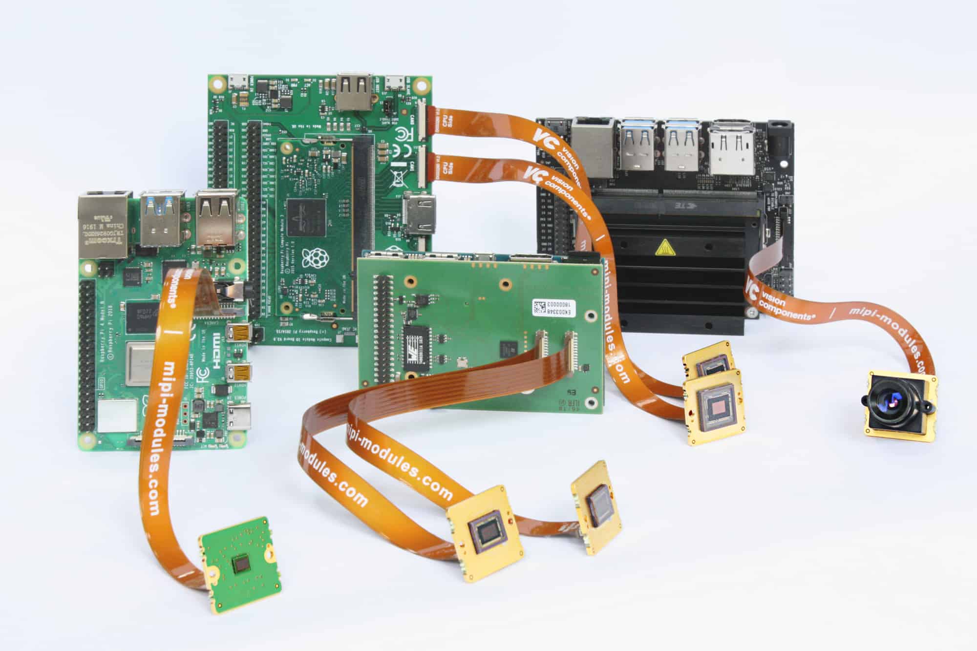
Rigid Flex PCB Applications
Some examples of products using rigid flex PCBs include:
Aerospace and Defense
- Missiles – Withstands vibration while saving space
- Radars – Complex antennas with tight folds and bends
- Avionics – Rugged connections between electronics
Medical
- Hearing aids – Bends to fit in ear canal
- Pacemakers – Flexible connections to sensors conform to body
- Patient monitors – Integrated cabling and sensors
Consumer Electronics
- Cellphones – Allows folding while embedding antennas
- Laptops – Interconnects for clamshell housing
- Cameras – Stable platform with flexible harness
Industrial
- Robotics – Flexible connections for moving joints
- Automation – Tight cabling around machinery
Automotive
- Sensors – Reliable in harsh temperature and vibration
- Infotainment – Hidden cabling within dash
- Lighting – Conforms to curved headlamps and tail lights
With rigid flex PCBs’ space savings and mechanical flexibility, they continue finding new applications across many industries.
Rigid Flex PCB Design and Manufacturing FQA
What are some typical layer counts for rigid flex PCBs?
Rigid layers typically range from 2 to 30 while flex layers are usually 2 to 8. High layer counts are possible but increase complexity and cost. Common configurations are 4-6 layers for rigid and 2 layers for flex sections.
What are recommended minimum bend radii for flex?
As a rule of thumb, the minimum bend radius should be at least 3 times the flex thickness for occasional bends, or 10 times for applications with dynamic flexing. This prevents metal fatigue and dielectric cracking over repeated bending cycles.
How are components assembled on rigid flex PCBs?
SMT components are assembled on rigid portions using standard surface mount equipment. Through-hole components or connectors can be manually soldered or selectively wave soldered. Additional adhesives may be used to strengthen solder joints in high vibration environments.
What design factors improve flex section reliability?
Gradual curves, corner chamfers, tear-drop vias, copper thickness builds, and adhesive enhancements help prevent conductor cracking and dielectric tears in dynamic flex areas. Stiffeners also relieve stress from concentrated flex zones.
How accurate is layer-to-layer alignment on rigid flex PCBs?
With advanced lamination processes, alignment between layers can reach +/- 0.075mm (3 mil) or better. Tight tolerances ensure reliable interconnections between layers during flexing motions.


Leave a Reply