Printed circuit boards (PCBs) are essential components in most electronic devices. They provide the mechanical structure and electrical connections between components. There are two main types of PCBs – rigid and flex. Understanding the differences between these two types of PCBs can help designers select the best option for their application.
What is a Rigid PCB?
A rigid PCB is the more common and traditional type of PCB. As the name suggests, rigid PCBs retain their shape and do not flex. The board material is typically made of rigid laminated fiberglass. Here are some key characteristics of rigid PCBs:
Materials
- The base material is typically FR-4 glass epoxy laminate. This provides mechanical rigidity and dimensional stability.
- The copper traces are etched or printed onto the board.
- A soldermask is applied over the traces for insulation and prevention of shorts.
- Silkscreen legend prints out component names and values.
- Vias and plated through holes (PTHs) allow connections between layers.
- Stiffeners can be added for structural support.
Properties
- Retains its shape – does not flex or bend.
- More durable and resistant to stresses.
- Allows for smaller trace sizes and spacing.
- Can accommodate more layers – up to 30+ layers.
- Heavier and thicker than flex PCBs.
- Requires connectors for flexibility between PCBs.
Applications
- Consumer electronics – laptops, PCs, TVs, etc.
- Automotive electronics.
- Industrial equipment.
- High density interconnects.
- Stable and durable applications that do not require flexing.
Manufacturing
- Photolithographic processes used to etch copper layers.
- Drilling used to create vias and PTHs.
- Automated assembly can place components.
- Soldering makes electrical connections.
- Able to manufacture small trace sizes and spacing.
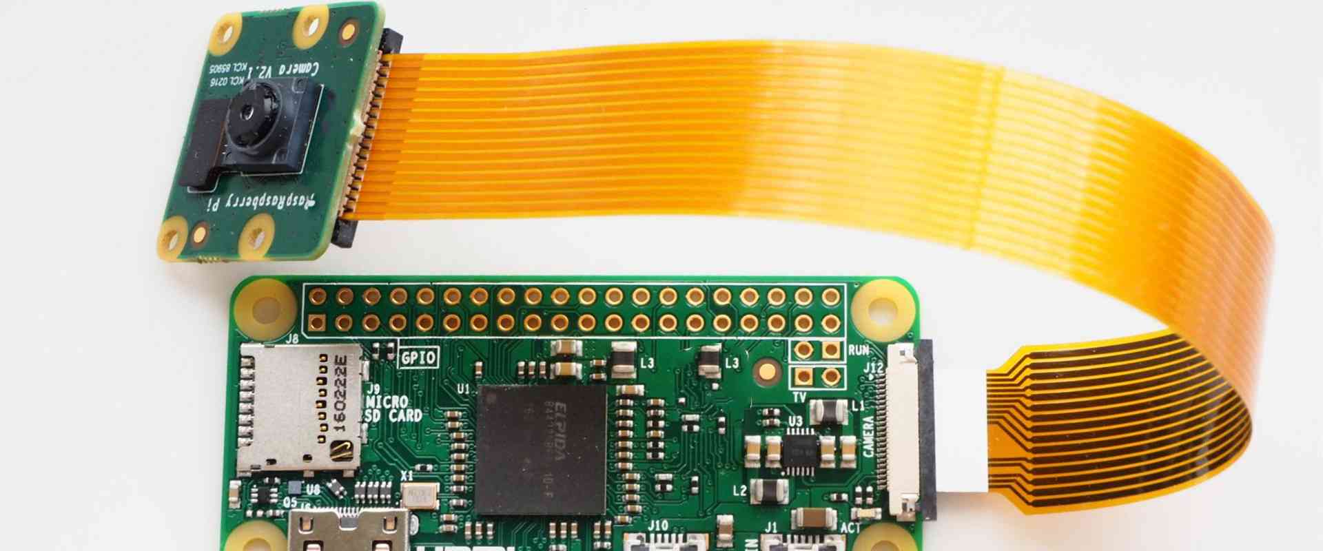
What is a Flex PCB?
A flex PCB can bend, curve, fold or flex. They are made of flexible dielectric materials like polyimide. Here are some key properties of flex PCBs:
Materials
- Base material is a flexible polymer like polyimide or polyester. This allows the board to flex without damage.
- Adhesive layers bond the conductor layers.
- Etched copper foil provides the conductive traces.
- Coverlay added for insulation and marking.
Properties
- Can flex and bend repeatedly.
- Dynamic and movable.
- Thinner, lighter and more flexible than rigid PCBs.
- Limited in number of layers – typically 1 to 6 layers.
- Not as durable or resistant to stresses.
- Larger minimum trace sizes and spacing.
Applications
- Wearable electronics – watches, fitness trackers.
- Medical devices.
- Robotics and mechanisms.
- Avoid wire harnesses and connectors.
- Vibration prone environments.
- Applications requiring dynamic movement and flexing.
Manufacturing
- Etching done on thin flexible metal foils.
- Adhesive bonding used instead of lamination.
- Plated holes allow connections between layers.
- More limited in trace spacing and sizes.
- Requires special handling during assembly.
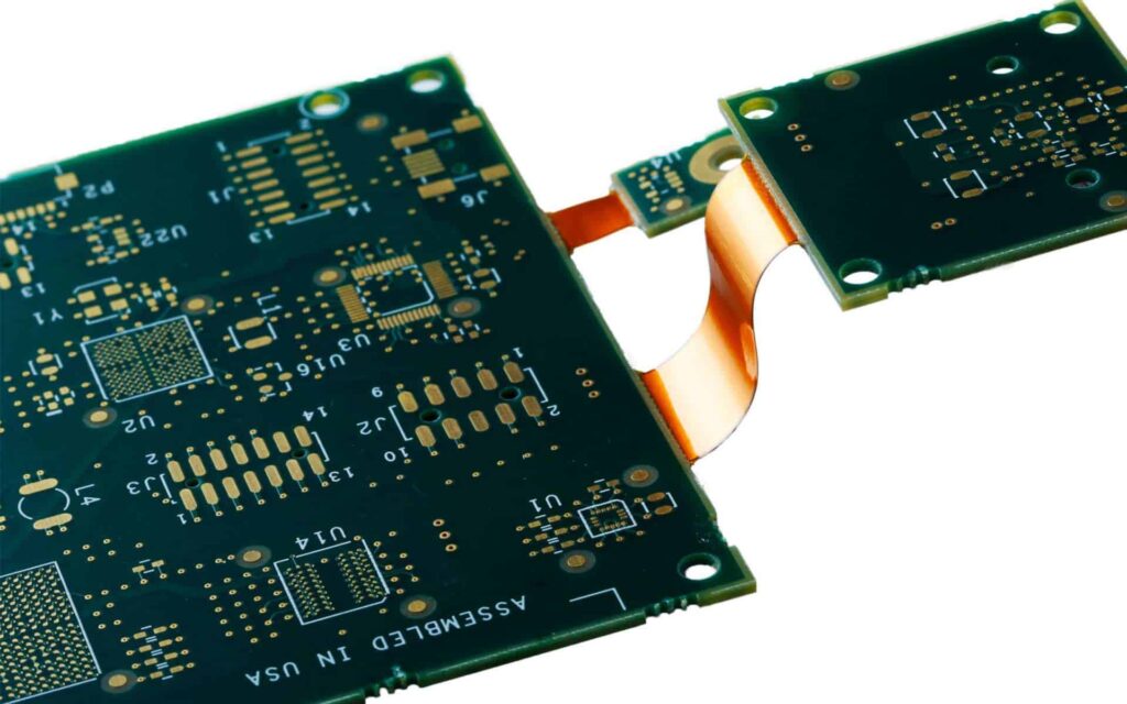
Rigid-Flex PCBs
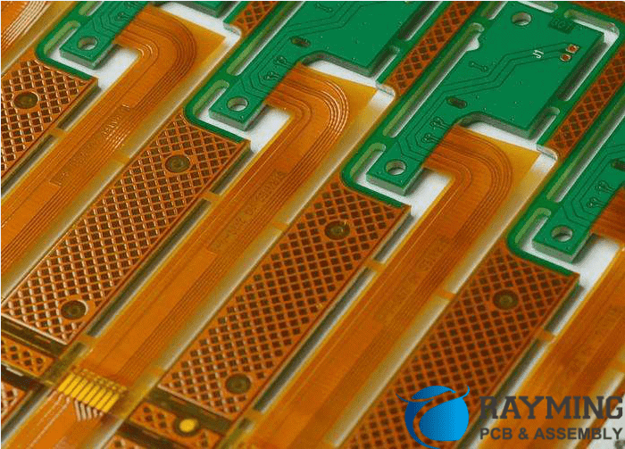
Rigid-flex PCBs combine both rigid and flex materials in one board. This allows designers to integrate both rigid and dynamic flexible sections:
- Can have multiple rigid sections interconnected by flex sections.
- Folding regions and hinges use flexible material.
- Dynamic sections use flex PCB areas.
- Rigid sections allow high density components and traces.
- Allows both 3D packaging and dynamic flexing.
- Used in advanced electronics like flip phones.
Here is a comparison table highlighting some of the differences between rigid and flex PCBs:
| Parameter | Rigid PCB | Flex PCB |
|---|---|---|
| Base Material | FR4, CEM | Polyimide, Polyester |
| Flexibility | None | Dynamic flexing |
| Number of layers | Up to 30+ | 1 to 6 typically |
| Trace spacing/size | Small | Larger minimums |
| Durability | High | Lower |
| Weight | Heavier | Lighter |
| Applications | Consumer electronics, high density | Wearables, mechanisms |
When to Use Rigid vs Flex PCBs?
Here are some guidelines on when to use rigid or flex PCBs:
When to use rigid PCBs:
- High density component mounting and small traces needed.
- Very thin traces and spacing required.
- Multilayer board with 6 or more layers required.
- Static application without flexing or bending.
- Durable applications with vibration or shock.
- Heavier components being mounted.
- Lower overall costs at high volumes.
When to use flex PCBs:
- Dynamic or repeated bending needed.
- Movement required in the application.
- 3D form factor and compact design needed.
- Production volumes will be low to medium.
- Vibration reduction is needed.
- Weight reduction is critical.
- Design changes may be frequent.
- Cost is lower at prototype and low volume stages.
When to use rigid-flex PCBs:
- When a design needs both rigid and flex areas on one board.
- To integrate rigid high density regions with dynamic flexing regions.
- Allowing a PCB to conform to a 3D shape.
- When folding or hinging actions are needed on a PCB.
- Avoiding connectors between separate rigid and flex PCBs.
Design Considerations
Here are some of the design considerations when working with rigid and flex PCBs:
For rigid PCBs:
- Component placement density and routing channels.
- Small via sizes and trace widths available.
- Controlled impedance traces if needed.
- Large continuous ground planes.
- Thermal management of components generating heat.
- Mounting and fastening holes for stability.
- High frequency signals, antennas, or EMI control.
- Number of conductive layers required.
For flex PCBs:
- Dynamic bending zones identified.
- Avoiding sharp flexing radii.
- Minimize traces crossing bend areas.
- Adhesive choices at folding sections.
- Trace widths matched to flex requirements.
- Strain relief shapes designed in.
- Component attachments and pads anchored.
- Copper thickness matched to flexibility needs.
For rigid-flex PCBs:
- Determine rigid and flex section outlines.
- Trace routing at transitions between sections.
- Impedance matching at rigid-flex boundaries.
- Layer planning for inner layer routing.
- Folding radius and sequence.
- Connectors or other termination needed.
- Bridging components across sections.
Careful design is needed to account for thermal expansion, dynamic bending cycles, component loads, and electrical connections when utilizing rigid-flex PCBs.
PCB Design and Fabrication Notes
Here are some best practice notes for designing and fabricating rigid and flex PCBs:
For rigid PCBs:
- Use smaller grid sizes for increased routing density.
- Utilize vias-in-pad for connections underneath components.
- Include thermal reliefs for plane connections at pads.
- Use blind and buried vias to optimize routing between layers.
- Include test points for validation and debugging.
- Specify trace finished that match the application – ENIG for example.
- Work closely with fabricators to design DFM-optimized boards.
For flex PCBs:
- Use teardrop pads for anchoring to the flexible substrate.
- Avoid acids that can etch away adhesive layers when cleaning.
- Remove all copper from flexible bending areas.
- Specify covers to prevent additional handling damage.
- Use fiducials or tooling holes to align layers.
- Test or prototype dynamic bending conditions.
- Provide precise mechanical drawings of flexed states.
For rigid-flex PCBs:
- Clearly outline the rigid and flex sections.
- Indicate board thickness changes between sections.
- Note preferred bending direction and sequence.
- Determine if edge plating is required.
- Extra protection may be needed during handling and assembly.
- Impedance matching and stacking sequence is key at transitions.
- Validate layout with designer, fabricator and assembler early.
Thorough communication between the design team and manufacturers will result in the best rigid or flex PCB outcomes.
Applications and Examples
Here are some examples of how rigid and flex PCBs are utilized:
- Wearable fitness trackers and smartwatches use narrow flexible PCBs that wrap around the wrist. This allows dynamic motion sensing and display viewing.
- Medical devices like hearing aids package components on thin flex circuits to fit into earpieces comfortably and safely. The flex PCB traces survive repeated bending cycles.
- Laptops integrate rigid multilayer PCBs for high density component mounting and routing. Connectors attach the rigid boards to peripheral components like keyboards.
- Robotics use rigid PCBs for motor drives and control components. Flex PCBs connect moving joints and minimize wiring harnesses.
- Cell phones contain multilayer rigid boards for computing, memory and RF modules. Flex PCBs attach and wrap around displays, buttons, batteries, and mechanisms.
- Consumer appliances like microwaves have rigid PCBs safely mounted with high voltage components and shielded compartments away from user areas.
- Automotive camera modules for surround vision mount camera sensors rigidly on small PCBs. Flex PCBs connect between movable modules while avoiding wiring harnesses.
Frequently Asked Questions
Here are some common FAQs about rigid and flex PCBs:
Q: How are rigid PCBs manufactured?
Rigid PCBs use photolithographic processes to image the trace patterns onto laminated sheets of fiberglass and copper foil. The unneeded copper is etched away, while plated through holes (PTHs) and vias create connections between layers. Multilayer boards are laminated together under heat and pressure.
Q: What are some key properties of polyimide flex PCB material?
Polyimide is a high temperature polymer that possesses some key properties for flex PCBs:
- High chemical resistance to solvents and acids
- Withstands continuous temperatures up to 300°C
- High tensile strength for repeated flexing
- Low coefficient of thermal expansion for reliability
- Good dielectric properties and insulation
Q: What are some ways rigid and flex PCBs are joined together?
Some methods for combining rigid and flex PCB materials:
- Adhesive lamination using bondply layers
- Soldered connections at component pads
- Board-to-board connectors
- Conductive adhesives like anisotropic films
- Plated half-etched tabs that overlay both sections
- Mechanical fixtures like clamps or screws
Q: How many bend cycles can flex PCBs support?
The flex life depends heavily on the bend radius. Tighter radii induce higher strains. Here are some typical bend cycle lifetimes:
- For 2mm bend radius: ~ 50,000 cycles
- For 5mm bend radius: ~ 100,000 cycles
- For 10mm bend radius: ~ 500,000 cycles
The design should aim for the largest bend radius possible for maximum cycling life.
Q: What are some methods for rigid and flex PCB design?
Some design methods include:
- 2D drawings, often with views of the flexed states
- 3D CAD models showing assembled configurations
- PCB layout tools like Altium and Cadence with rigid-flex design features
- Specialized rigid-flex design tools like Mentor’s Capital and CADIFLEX
- Mechanical simulation of stresses and bending
Close communication with fabrication partners is critical to ensure manufacturability.


Leave a Reply