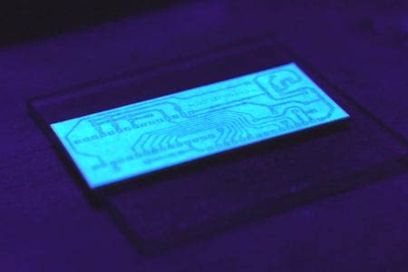
What is a Presensitized PCB?
A presensitized PCB, also known as a photosensitive PCB or pre-coated PCB, is a type of printed circuit board that comes with a light-sensitive photoresist layer pre-applied to its surface. This photoresist layer is a crucial component in the PCB manufacturing process, as it allows for the precise transfer of the circuit pattern onto the copper layer of the board.
Composition of a Presensitized PCB
A typical presensitized PCB consists of the following layers:
- Substrate: The base material of the PCB, usually made of fiberglass or epoxy.
- Copper layer: A thin layer of copper foil laminated onto the substrate, which will form the conductive paths of the circuit.
- Photoresist layer: A light-sensitive polymer coating applied on top of the copper layer.
- Protective film: A transparent film that covers the photoresist layer to protect it from damage and contamination.
Manufacturing Process of Presensitized PCBs
The manufacturing process of presensitized PCBs involves several steps, each critical to ensuring the quality and functionality of the final product.
Step 1: Substrate Preparation
The first step in the manufacturing process is to prepare the substrate. The substrate material, typically FR-4 (a type of fiberglass), is cut to the desired size and shape. The surface of the substrate is then cleaned and treated to ensure proper adhesion of the copper layer.
Step 2: Copper Lamination
A thin layer of copper foil is laminated onto the substrate using heat and pressure. The copper foil is typically available in various thicknesses, depending on the requirements of the specific application. The most common copper thicknesses are 1 oz (35 μm) and 2 oz (70 μm).
Step 3: Photoresist Application
The photoresist layer is then applied to the copper surface of the PCB. This is done using a process called curtain coating, where the liquid photoresist is poured onto the moving PCB, forming a uniform layer. The photoresist is then dried and cured using heat.
Step 4: Protective Film Application
After the photoresist layer is cured, a protective film is applied on top of it. This film serves two purposes: protecting the photoresist from damage during handling and storage, and acting as a template for the circuit pattern exposure.
Step 5: Packaging and Storage
Once the presensitized PCBs are manufactured, they are packaged in moisture-proof bags or boxes to protect them from environmental factors such as humidity and light. The boards are then stored in a cool, dry place until they are ready to be used.

Advantages of Presensitized PCBs
Presensitized PCBs offer several advantages over conventional PCBs, making them a popular choice for both hobbyists and professionals.
- Ease of use: With the photoresist layer pre-applied, presensitized PCBs eliminate the need for manual photoresist application, saving time and effort.
- Consistency: The factory-controlled application of the photoresist layer ensures a uniform thickness and quality, reducing the chances of defects or inconsistencies.
- Cost-effectiveness: Presensitized PCBs are generally more affordable than conventional PCBs, as they streamline the manufacturing process and reduce labor costs.
- Improved resolution: The pre-applied photoresist layer enables higher resolution circuit patterns, allowing for the creation of more complex and compact designs.
- Faster turnaround: By simplifying the PCB manufacturing process, presensitized PCBs can be produced more quickly, reducing lead times and accelerating project completion.

Applications of Presensitized PCBs
Presensitized PCBs find applications in a wide range of industries and projects, from consumer electronics to aerospace. Some common applications include:
- Prototyping: Presensitized PCBs are ideal for creating prototypes and testing new designs, as they allow for quick and easy fabrication of custom circuit boards.
- Small-scale production: For low-volume production runs, presensitized PCBs offer a cost-effective solution, as they eliminate the need for expensive setup costs associated with conventional PCB manufacturing methods.
- Educational purposes: Many educational institutions use presensitized PCBs to teach students about electronics and PCB design, as they provide a hands-on learning experience.
- Hobbyist projects: DIY enthusiasts and hobbyists often use presensitized PCBs for their personal projects, such as building custom electronic devices or experimenting with new circuit designs.

Choosing the Right Presensitized PCB
When selecting a presensitized PCB for your project, there are several factors to consider to ensure the best performance and compatibility.
Substrate Material
The most common substrate material for presensitized PCBs is FR-4, a fiberglass-reinforced epoxy laminate. FR-4 offers good mechanical strength, electrical insulation, and thermal stability. However, for high-frequency or high-temperature applications, other substrate materials like Rogers or polyimide may be more suitable.
Copper Thickness
The thickness of the copper layer on a presensitized PCB is typically expressed in ounces (oz) per square foot. Common copper thicknesses include 1 oz (35 μm) and 2 oz (70 μm). Thicker copper layers are generally used for high-current or high-power applications, while thinner layers are suitable for general-purpose use.
Photoresist Type
There are two main types of photoresist used in presensitized PCBs: positive and negative. Positive photoresist becomes soluble when exposed to light, while negative photoresist becomes insoluble. The choice between positive and negative photoresist depends on the specific requirements of your project, such as the desired circuit pattern and the exposure method used.
Exposure Method
Presensitized PCBs can be exposed using various methods, including UV light, laser, and direct imaging. UV exposure is the most common method, using a photomask and a UV light source to transfer the circuit pattern onto the photoresist. Laser exposure and direct imaging offer higher resolution and precision but are more expensive.
Manufacturer Reputation
When choosing a presensitized PCB manufacturer, it is essential to consider their reputation, quality control processes, and customer support. Look for manufacturers with a proven track record of producing high-quality boards and providing reliable service.
Working with Presensitized PCBs
Once you have selected the appropriate presensitized PCB for your project, the next step is to expose and develop the circuit pattern onto the board. This process involves several key steps.
Step 1: Artwork Preparation
The first step is to create the artwork for your circuit pattern. This can be done using PCB design software, such as Eagle, KiCad, or Altium Designer. The artwork should be created according to the manufacturer’s specifications, including the minimum feature size and clearance requirements.
Step 2: Photomask Creation
The next step is to create a photomask based on the artwork. A photomask is a transparent sheet with the circuit pattern printed on it in black ink. The photomask is used to selectively block light during the exposure process, transferring the circuit pattern onto the photoresist. Photomasks can be created using various methods, such as inkjet printing, laser printing, or photoplotter printing.
Step 3: Exposure
Once the photomask is ready, the presensitized PCB is placed in an exposure unit, with the photomask on top of it. The board is then exposed to UV light for a specific duration, depending on the photoresist type and thickness. The UV light passes through the transparent areas of the photomask, causing a chemical change in the photoresist.
Step 4: Development
After exposure, the PCB is removed from the exposure unit and placed in a developing solution. The developing solution dissolves the exposed (for positive photoresist) or unexposed (for negative photoresist) areas of the photoresist, revealing the copper layer underneath. The development time and temperature are critical factors in ensuring a clean and accurate pattern transfer.
Step 5: Etching
Once the photoresist is developed, the PCB is placed in an etching solution, typically ferric chloride or ammonium persulfate. The etching solution removes the copper from the areas not protected by the photoresist, leaving behind the desired circuit pattern. The etching time and temperature must be carefully controlled to avoid over-etching or under-etching.
Step 6: Stripping and Cleaning
After etching, the remaining photoresist is stripped from the PCB using a stripping solution. The board is then cleaned and dried, ready for the next steps in the manufacturing process, such as drilling, solder mask application, and silkscreen printing.
Troubleshooting Common Issues
Despite the ease of use and consistency offered by presensitized PCBs, issues can still arise during the manufacturing process. Some common problems and their solutions include:
-
Incomplete or patchy exposure: This can be caused by a weak UV light source, incorrect exposure time, or a damaged photomask. To resolve this issue, ensure that the exposure unit is functioning correctly, adjust the exposure time, and inspect the photomask for any defects.
-
Over-development or under-development: If the developing time is too long or too short, it can result in an inaccurate pattern transfer. Follow the manufacturer’s recommendations for developing time and temperature, and adjust as needed based on the results.
-
Over-etching or under-etching: Similar to development issues, incorrect etching time or temperature can lead to problems with the final circuit pattern. Monitor the etching process closely and adjust the parameters as needed to achieve the desired results.
-
Poor adhesion of photoresist: If the photoresist does not adhere properly to the copper layer, it can cause issues during exposure and development. Ensure that the PCB surface is clean and free of contaminants before applying the photoresist, and follow the manufacturer’s storage and handling guidelines.
-
Contamination or damage to the photoresist: Dust, fingerprints, or scratches on the photoresist can cause defects in the final circuit pattern. Handle the presensitized PCBs with care, and store them in a clean, dry environment.
Future Trends in Presensitized PCBs
As the electronics industry continues to evolve, presensitized PCBs are also expected to advance and adapt to new challenges and requirements. Some future trends in presensitized PCBs include:
-
Higher resolution and smaller feature sizes: With the increasing demand for miniaturization and high-density circuits, presensitized PCBs will need to support finer pitch sizes and smaller vias.
-
Advanced substrate materials: New substrate materials, such as high-frequency laminates and flexible substrates, will be developed to meet the needs of emerging applications, such as 5G communication and wearable electronics.
-
Environmentally friendly processes: As environmental concerns grow, there will be a push towards more eco-friendly manufacturing processes, including the use of non-toxic photoresists and etching solutions.
-
Increased automation: To improve efficiency and reduce costs, presensitized PCB manufacturing will likely see increased automation, from artwork generation to exposure and development.
-
Integration with additive manufacturing: The combination of presensitized PCBs with additive manufacturing techniques, such as 3D printing, could enable the creation of complex, three-dimensional circuits and devices.
Frequently Asked Questions (FAQ)
-
What is the shelf life of presensitized PCBs?
Presensitized PCBs typically have a shelf life of 6 to 12 months when stored properly in a cool, dry, and dark environment. However, it is always best to consult the manufacturer’s guidelines for specific storage and handling instructions. -
Can presensitized PCBs be used for multilayer boards?
Yes, presensitized PCBs can be used to create multilayer boards. The process involves laminating multiple presensitized PCBs together, with insulating layers between them, and then exposing, developing, and etching each layer separately. -
Are presensitized PCBs suitable for high-frequency applications?
Presensitized PCBs can be used for high-frequency applications, provided that the appropriate substrate material and copper thickness are selected. High-frequency laminates, such as Rogers or Teflon, offer better dielectric properties and signal integrity compared to standard FR-4 substrates. -
How do I select the right photoresist type for my project?
The choice between positive and negative photoresist depends on factors such as the desired circuit pattern, the exposure method, and the etching process. In general, positive photoresist is more common and offers better resolution, while negative photoresist is more resistant to harsh etching solutions. -
Can I reuse a presensitized PCB if I make a mistake during exposure or development?
In most cases, if a mistake is made during exposure or development, the presensitized PCB cannot be reused. However, if the mistake is caught early enough and the photoresist is not completely developed, it may be possible to strip the photoresist and start over with a new layer.
Conclusion
Presensitized PCBs have revolutionized the printed circuit board manufacturing process, offering a cost-effective, consistent, and user-friendly solution for creating custom circuit boards. By understanding the composition, manufacturing process, and key considerations when working with presensitized PCBs, engineers, hobbyists, and educators can harness their potential to bring their electronic projects to life.
As the electronics industry continues to evolve, presensitized PCBs are expected to advance and adapt, supporting higher resolution, new substrate materials, and more environmentally friendly processes. By staying informed about these trends and best practices, users can ensure that they are making the most of this versatile and powerful technology.
Whether you are a seasoned professional or a beginner in the world of PCBs, presensitized PCBs offer a compelling option for creating high-quality, custom circuit boards with ease. With the right knowledge and tools, the possibilities are endless.
| Characteristic | Presensitized PCB | Conventional PCB |
|---|---|---|
| Photoresist Application | Pre-applied by manufacturer | Applied manually |
| Consistency | High, factory-controlled | Variable, depends on operator skill |
| Cost | Lower, streamlined process | Higher, more labor-intensive |
| Resolution | Higher, finer pitch possible | Lower, limited by manual application |
| Turnaround Time | Faster, simplified process | Slower, more complex process |


Leave a Reply