What is Photolithography?
Photolithography, also known as optical lithography or UV lithography, is a process used in microfabrication to pattern parts of a thin film or the bulk of a substrate. It uses light to transfer a geometric pattern from a photomask to a light-sensitive chemical “photoresist” on the substrate. A series of chemical treatments then either engraves the exposure pattern into the material or enables deposition of a new material in the desired pattern upon the material underneath the photoresist.
Key Components of Photolithography
- Photoresist
- Photomask
- UV light source
- Developing solution
- Etching or deposition process
History of Photolithography
The concept of photolithography dates back to 1822 when Nicéphore Niépce invented a photographic process called heliography. However, it wasn’t until the 1950s that photolithography was used in the semiconductor industry. In 1955, Andrus and Bond at Bell Labs developed the first photolithographic process for patterning silicon wafers.
| Year | Development |
|---|---|
| 1822 | Nicéphore Niépce invents heliography |
| 1955 | Andrus and Bond develop photolithography for silicon wafers |
| 1960s | Photolithography becomes the dominant patterning technology in the semiconductor industry |
| 1970s | Resolution of photolithography reaches 1 μm |
| 1980s | Resolution of photolithography reaches 0.5 μm |
| 1990s | Resolution of photolithography reaches 0.25 μm |
| 2000s | Resolution of photolithography reaches sub-100 nm |

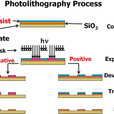
The Photolithography Process
The photolithography process consists of several steps:
- Wafer cleaning
- Photoresist application
- Soft baking
- Mask alignment and exposure
- Development
- Hard baking
- Etching or deposition
- Photoresist removal
1. Wafer Cleaning
The first step in the photolithography process is to clean the wafer thoroughly. This is done to remove any contaminants or particles that may affect the quality of the final product. The wafer is typically cleaned using a combination of chemical and physical methods, such as:
- Piranha solution (sulfuric acid and hydrogen peroxide)
- RCA clean (ammonium hydroxide, hydrogen peroxide, and water)
- Ultrasonic cleaning
2. Photoresist Application
After cleaning, a thin layer of photoresist is applied to the wafer surface. This is typically done using a spin coating process, where the wafer is rapidly rotated while the photoresist is dispensed onto the center of the wafer. The centrifugal force spreads the photoresist evenly across the surface, creating a uniform layer.
Types of Photoresist
There are two main types of photoresist:
- Positive photoresist: When exposed to light, the exposed areas become soluble in the developer solution.
- Negative photoresist: When exposed to light, the exposed areas become insoluble in the developer solution.
3. Soft Baking
After the photoresist is applied, the wafer undergoes a soft baking process. This is done to remove any remaining solvents from the photoresist and to improve adhesion to the wafer surface. Soft baking is typically performed at temperatures between 90-100°C for 30-60 seconds.
4. Mask Alignment and Exposure
The next step is to align the photomask with the wafer and expose it to UV light. The photomask contains the desired pattern that will be transferred to the photoresist. The alignment process is critical to ensure that the pattern is transferred accurately.
During exposure, UV light passes through the transparent areas of the photomask and interacts with the photoresist. In positive photoresist, the exposed areas become soluble, while in negative photoresist, the exposed areas become insoluble.
5. Development
After exposure, the wafer is immersed in a developing solution. This solution selectively removes either the exposed (positive photoresist) or unexposed (negative photoresist) areas of the photoresist, revealing the desired pattern on the wafer surface.
6. Hard Baking
Following development, the wafer undergoes a hard baking process. This is done to improve the adhesion and thermal stability of the remaining photoresist. Hard baking is typically performed at temperatures between 120-180°C for 20-30 minutes.
7. Etching or Deposition
With the desired pattern now present on the wafer surface, the next step is to transfer this pattern to the underlying material. This can be done through etching or deposition processes.
- Etching: The exposed areas of the underlying material are removed using chemical or physical methods, such as wet etching or reactive ion etching (RIE).
- Deposition: New material is deposited onto the wafer surface, adhering only to the areas not protected by the photoresist. This can be done using techniques such as physical vapor deposition (PVD) or chemical vapor deposition (CVD).
8. Photoresist Removal
After the etching or deposition process is complete, the remaining photoresist is removed from the wafer surface. This is typically done using a combination of chemical and physical methods, such as:
- Oxygen plasma ashing
- Solvent stripping
- Piranha solution

Applications of Photolithography
Photolithography is a versatile process with numerous applications across various industries:
- Semiconductor industry: Fabrication of integrated circuits, microprocessors, and memory devices.
- MEMS (Micro-Electro-Mechanical Systems): Fabrication of sensors, actuators, and microfluidic devices.
- Optics: Fabrication of diffractive optical elements, waveguides, and microlens arrays.
- Biotechnology: Fabrication of microarrays, lab-on-a-chip devices, and biosensors.
- Nanotechnology: Fabrication of nanostructures, nanopatterns, and nanoimprint lithography templates.

Challenges and Future Developments
As the demand for smaller and more complex devices continues to grow, photolithography faces several challenges:
- Resolution limits: The minimum feature size that can be achieved with photolithography is limited by the wavelength of the light used. To overcome this, techniques such as immersion lithography and extreme ultraviolet (EUV) lithography are being developed.
- Overlay accuracy: As device dimensions shrink, the alignment and overlay accuracy between multiple lithography steps becomes increasingly critical.
- Cost: Advanced photolithography systems, such as EUV lithography tools, are extremely expensive, driving up the cost of fabrication.
Despite these challenges, photolithography remains the dominant patterning technology in the semiconductor industry. Ongoing research and development efforts aim to push the boundaries of resolution, improve overlay accuracy, and reduce costs.
Frequently Asked Questions (FAQ)
- What is the difference between positive and negative photoresist?
-
Positive photoresist becomes soluble in the developer solution when exposed to light, while negative photoresist becomes insoluble when exposed to light.
-
What is the purpose of soft baking in the photolithography process?
-
Soft baking is done to remove any remaining solvents from the photoresist and to improve adhesion to the wafer surface.
-
What is the role of the photomask in photolithography?
-
The photomask contains the desired pattern that will be transferred to the photoresist during the exposure step.
-
What is the difference between etching and deposition in the context of photolithography?
-
Etching removes material from the wafer surface in the areas not protected by the photoresist, while deposition adds new material to the wafer surface in the areas not protected by the photoresist.
-
What are some of the key challenges facing photolithography technology?
- Resolution limits, overlay accuracy, and high costs are some of the main challenges facing photolithography technology as device dimensions continue to shrink.
In conclusion, photolithography is a critical process in the fabrication of semiconductor devices, MEMS, and various other applications. By using light to transfer patterns from a photomask to a photoresist-coated wafer, photolithography enables the creation of complex, high-resolution structures. As the demand for smaller and more advanced devices grows, photolithography technology will continue to evolve to meet these challenges, driving innovation across numerous industries.


Leave a Reply