PCB Manufacturing Process Overview
The PCB manufacturing process can be broken down into three main stages:
- PCB Design & Engineering: Creating the PCB design files
- PCB Fabrication: Making the bare printed circuit board
- PCB Assembly: Soldering components onto the board
PCB Manufacturing Process Flow
| Step | Design & Engineering | Fabrication | Assembly |
|---|---|---|---|
| 1 | Schematic Capture | Drilling | Solder Paste Application |
| 2 | PCB Layout | Plating | Pick and Place |
| 3 | Design Rule Checks | Etching | Reflow Soldering |
| 4 | Gerber File Generation | Solder Mask Application | Inspection |
| 5 | Silkscreen | Testing | |
| 6 | Surface Finish |
PCB Design & Engineering
The first step in PCB manufacturing is creating the design files that will be used to fabricate and assemble the board. This involves several steps:
Schematic Capture
The schematic diagram is a symbolic representation of the circuit. It defines the electrical connections between components. Schematics are drawn in EDA (electronic design automation) software.
PCB Layout
Once the schematic is complete, the physical PCB layout is created in the EDA tool. Components are arranged on the board and copper traces are routed to make the connections defined in the schematic. The PCB layout must follow design rules for manufacturing.
Design Rule Checks (DRC)
The EDA software performs design rule checks to verify the PCB layout meets manufacturing specifications. This includes checks for minimum trace width and spacing, hole sizes, annular rings, etc. DRCs help ensure the board is manufacturable.
Gerber File Generation
After the layout is complete and passes DRC, the design is exported to Gerber format. Gerber is the standard file format for PCB fabrication. A separate Gerber file is generated for each layer of the board – copper, solder mask, silkscreen, drill data, etc.

PCB Fabrication
With the Gerber files, the bare PCB is fabricated. Fabrication involves several process steps:
Drilling
Holes are drilled in a bare copper-clad board. These include holes for through-hole components and vias to route traces between layers. Hole size and position is controlled by the drill file.
Plating
Copper is electroplated onto the board, building up the thickness of the traces and plating through the holes to connect the top and bottom layers.
Etching
A photoresist mask is applied over the copper and exposed with UV light to transfer the trace pattern. The unexposed photoresist is removed, and the unmasked copper is etched away. This leaves only the desired traces.
Solder Mask Application
A polymer solder mask is applied to cover the bare copper traces. This insulating layer prevents solder bridges and protects the traces. Solder mask is typically green, but other colors are available.
Silkscreen
A silkscreen legend is printed on the board to label components, show company logos, part numbers, etc. Silkscreen is usually white but can be other colors.
Surface Finish
A surface finish, such as HASL (hot air solder leveling), lead-free HASL, or ENIG (electroless nickel immersion gold) is applied to the exposed copper on the pads. The surface finish protects the copper and enhances solderability.

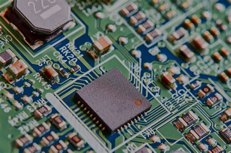
PCB Assembly
After fabrication, the components are soldered to the board. PCB assembly also involves multiple steps:
Solder Paste Application
Solder paste, a mixture of tiny solder spheres and flux, is applied to the pads on the board. The most common method is using a stencil and squeegee to deposit solder paste only on the pads.
Pick and Place
An automated pick and place machine picks up SMD components from reels or trays and places them onto the solder paste deposits on the pads. Placement is programmed based on the CAD data for the board.
Reflow Soldering
After components are placed, the board goes through a reflow oven. This heats the board in stages, activating the flux and melting the solder to form solder joints. The temperature profile is tightly controlled for reliable solder joints.
Inspection
After reflow, solder joints are inspected, either manually or using automated optical inspection (AOI) to check for defects like bridges, opens, or misaligned components.
Testing
Functional circuit testing verifies that the assembled board operates correctly. In-circuit testing (ICT) uses pogo pin fixtures to access test points and run diagnostics. Other functional tests may also be performed, depending on the product.

PCB Manufacturing Considerations
Several factors impact the PCB manufacturing process:
Board Complexity
More complex designs with finer pitch components, smaller vias, thinner traces, and higher layer counts require more advanced manufacturing capabilities. Fabricators are classified by the minimum feature sizes they can produce.
Material Selection
FR-4 is the most common base material for PCBs, but other substrates like polyimide, teflon, or metal core materials may be used for special applications. The material affects the processing parameters.
Quality & Reliability
Manufacturing a reliable board that meets quality and performance requirements involves controlling many variables in the fabrication and assembly process. This includes things like annular ring size, plating thickness, solder mask registration, and solder joint geometry.
Cost Drivers
PCB size, layer count, minimum feature sizes, surface finish, and testing requirements all impact the cost to manufacture the board. In general, smaller, simpler boards are less expensive. The tradeoff between cost and complexity must be managed.
PCB Manufacturing FAQ
What is the standard PCB thickness?
The most common PCB thickness is 1.6mm (0.062″), but thicknesses range from 0.4mm to 3.2mm or more. Thinner boards are often used in mobile devices, while thicker boards provide more mechanical strength.
What are the different types of vias in a PCB?
Through-hole vias go all the way through the board, while blind vias connect an outer layer to an inner layer, and buried vias connect two inner layers. Microvias are small vias, usually laser drilled.
What is the difference between HASL and ENIG surface finish?
Hot air solder leveling (HASL) is a low-cost finish where the pads are coated with solder. Electroless nickel immersion gold (ENIG) has a thin layer of gold over nickel, which protects the copper and provides good planarity for fine pitch components. ENIG is more expensive than HASL.
How long does it take to manufacture a PCB?
Fabrication time depends on the complexity of the board and the manufacturer’s capabilities. Simple 2-layer boards can be made in 1-2 days, while complex multilayer boards may take several weeks. Expedited turns are available for an additional cost.
What are the most common PCB assembly defects?
Some common assembly defects include tombstoning (one end of a component lifts up), bridging (solder shorts between pads), open solder joints, shifted or misaligned components, and insufficient solder fillets. Choosing a qualified contract manufacturer and having good DFM practices minimizes defects.


Leave a Reply