What are PCBs?
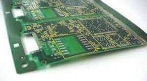
PCBs, or Printed Circuit Boards, are the backbone of modern electronics. They are the green boards that you find inside almost every electronic device, from smartphones and computers to televisions and medical equipment. PCBs are designed to mechanically support and electrically connect electronic components using conductive tracks, pads, and other features etched from copper sheets laminated onto a non-conductive substrate.
The Composition of PCBs
PCBs are typically composed of several layers:
- Substrate: This is the base material of the PCB, usually made of fiberglass or other insulating materials.
- Copper: Thin layers of copper foil are laminated onto the substrate. These copper layers are etched to create the conductive tracks and pads that connect the electronic components.
- Solder Mask: A protective layer that covers the copper traces, leaving only the pads and other areas that need to be soldered exposed.
- Silkscreen: A printed layer that adds text, logos, and other identifying marks to the PCB.
Types of PCBs
There are three main types of PCBs:
1. Single-Layer PCBs
Single-layer PCBs have copper traces on only one side of the substrate. They are the simplest and most cost-effective type of PCB, suitable for basic electronic circuits.
2. Double-Layer PCBs
Double-layer PCBs have copper traces on both sides of the substrate. They offer more design flexibility and higher component density compared to single-layer PCBs. Double-layer PCBs are commonly used in more complex electronic devices.
3. Multi-Layer PCBs
Multi-layer PCBs have three or more layers of copper traces. They are used in highly complex electronic systems that require high component density and signal integrity. Multi-layer PCBs are more expensive to manufacture than single- or double-layer PCBs.
| PCB Type | Layers | Complexity | Cost |
|---|---|---|---|
| Single-Layer | 1 | Low | Low |
| Double-Layer | 2 | Medium | Medium |
| Multi-Layer | 3+ | High | High |

PCB Design Process
The PCB design process involves several steps:
1. Schematic Design
The first step is to create a schematic diagram of the electronic circuit. This diagram shows how the components are connected electrically, without regard for their physical layout.
2. Component Placement
Once the schematic is complete, the components are placed on the virtual PCB layout. The placement is optimized for signal integrity, manufacturability, and other factors.
3. Routing
The copper traces are then routed to connect the components according to the schematic. The routing must follow design rules to ensure proper signal integrity and manufacturability.
4. Design Rule Check (DRC)
The PCB layout is checked against a set of design rules to ensure that it meets manufacturing requirements and standards.
5. Gerber File Generation
Once the PCB layout is finalized, Gerber files are generated. These files contain all the information needed to manufacture the PCB, including the copper layers, solder mask, and silkscreen.

PCB Manufacturing Process
The PCB manufacturing process involves several steps:
1. PCB Fabrication
The PCB substrate is cut to size, and the copper layers are laminated onto it. The copper is then etched to create the conductive tracks and pads according to the Gerber files.
2. Solder Mask Application
The solder mask is applied to the PCB, covering the copper traces and leaving only the pads and other areas that need to be soldered exposed.
3. Silkscreen Printing
The silkscreen layer is printed onto the PCB, adding text, logos, and other identifying marks.
4. Surface Finish Application
A surface finish, such as HASL (Hot Air Solder Leveling) or ENIG (Electroless Nickel Immersion Gold), is applied to the exposed copper to protect it from oxidation and enhance solderability.
5. Electrical Testing
The PCB is electrically tested to ensure that all connections are correct and there are no short circuits or open circuits.

PCB Assembly Process
The PCB assembly process involves several steps:
1. Solder Paste Application
Solder paste is applied to the pads on the PCB using a stencil or screen printing process.
2. Component Placement
The electronic components are placed onto the PCB, either manually or using automated pick-and-place machines.
3. Reflow Soldering
The PCB with the placed components is passed through a reflow oven, which melts the solder paste and creates a permanent electrical and mechanical connection between the components and the PCB.
4. Inspection
The assembled PCB is inspected visually and with automated optical inspection (AOI) systems to ensure that all components are correctly placed and soldered.
5. Functional Testing
The assembled PCB is functionally tested to ensure that it performs as intended.
Advantages of PCBs
PCBs offer several advantages over other methods of connecting electronic components:
- Reliability: PCBs provide a stable and reliable platform for electronic components, reducing the risk of loose connections and short circuits.
- Repeatability: PCBs can be mass-produced with consistent quality, ensuring that each board performs identically.
- Size: PCBs allow for high component density, enabling the creation of compact and lightweight electronic devices.
- Cost: PCBs are cost-effective, especially when produced in large quantities.
Applications of PCBs
PCBs are used in virtually every electronic device, including:
- Smartphones
- Computers
- Televisions
- Medical equipment
- Automotive electronics
- Industrial control systems
- Aerospace and defense systems
Frequently Asked Questions (FAQ)
1. What is the difference between a PCB and a breadboard?
A breadboard is a temporary prototyping tool used to build and test electronic circuits without soldering. PCBs, on the other hand, are permanent boards that provide a stable and reliable platform for electronic components.
2. Can I design my own PCB?
Yes, you can design your own PCB using PCB design software such as Altium Designer, KiCad, or Eagle. However, designing a PCB requires knowledge of electronic circuits and PCB design principles.
3. How much does it cost to manufacture a PCB?
The cost of manufacturing a PCB depends on several factors, such as the size of the board, the number of layers, the quantity ordered, and the turnaround time. Simple single-layer PCBs can cost as little as a few dollars per board, while complex multi-layer PCBs can cost hundreds of dollars per board.
4. What is the lead time for PCB manufacturing?
The lead time for PCB manufacturing depends on the complexity of the board and the manufacturer’s workload. Simple PCBs can be manufactured in a few days, while complex PCBs can take several weeks.
5. Can PCBs be recycled?
Yes, PCBs can be recycled to recover valuable materials such as gold, silver, and copper. However, PCB Recycling is a complex process that requires specialized equipment and expertise to ensure that hazardous materials are properly handled and disposed of.
Conclusion
PCBs are the foundation of modern electronics, providing a reliable and cost-effective platform for connecting electronic components. Understanding the fundamentals of PCBs, including their composition, types, design process, manufacturing process, and assembly process, is essential for anyone involved in electronics design or manufacturing.
As technology continues to advance, the demand for PCBs will only increase. By mastering the fundamentals of PCBs, you can position yourself to take advantage of the many opportunities in this exciting and dynamic field.


Leave a Reply