Understanding PCB Capacitance
Printed Circuit Board (PCB) design involves various aspects, one of which is managing the capacitance between traces and planes. PCB capacitance plays a crucial role in determining the performance, signal integrity, and electromagnetic compatibility of electronic circuits. In this article, we will delve into the concept of PCB trace to plane capacitance and explore the formula used to calculate it.
What is PCB Capacitance?
PCB capacitance refers to the ability of a PCB to store electrical charge between its conductive layers. It is an inherent property of PCBs due to the presence of dielectric materials and the proximity of conductive traces and planes. Capacitance exists between any two conductive surfaces separated by an insulating material, and PCBs are no exception.
Importance of PCB Capacitance
Understanding and managing PCB capacitance is essential for several reasons:
-
Signal Integrity: Capacitance between traces and planes can affect the propagation of signals through the PCB. It can cause signal distortion, reflections, and crosstalk, which can degrade the overall signal integrity of the system.
-
Electromagnetic Compatibility (EMC): PCB capacitance can impact the electromagnetic compatibility of the circuit. Unintended capacitance can lead to unwanted coupling between traces, resulting in electromagnetic interference (EMI) and potential compliance issues.
-
Impedance Matching: Proper management of PCB capacitance is crucial for maintaining the characteristic impedance of transmission lines. Mismatched impedances can cause signal reflections and degrade the signal quality.
-
Power Distribution Network (PDN) Design: Capacitance between power planes and ground planes forms a part of the PDN. Accurately estimating and controlling this capacitance is necessary for designing a stable and efficient power distribution system.
Factors Affecting PCB Trace to Plane Capacitance
Several factors influence the capacitance between a PCB trace and a plane:
-
Dielectric Material: The dielectric material used in the PCB, such as FR-4, determines the permittivity (ε) of the insulating layer. Higher permittivity materials result in higher capacitance.
-
Dielectric Thickness: The thickness of the dielectric layer between the trace and the plane directly affects the capacitance. Thinner dielectric layers lead to higher capacitance values.
-
Trace Geometry: The width, length, and thickness of the trace impact its capacitance to the plane. Wider and longer traces have higher capacitance compared to narrower and shorter traces.
-
Plane Area: The size of the plane area underneath the trace influences the capacitance. A larger plane area results in higher capacitance.
-
Trace-to-Plane Spacing: The distance between the trace and the plane, often determined by the PCB Stackup, affects the capacitance. Closer spacing leads to higher capacitance.

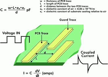
PCB Trace to Plane Capacitance Formula
The capacitance between a PCB trace and a plane can be calculated using the following formula:
C = (ε * ε0 * A) / d
Where:
– C is the capacitance in farads (F)
– ε is the relative permittivity of the dielectric material (unitless)
– ε0 is the permittivity of free space, which is approximately 8.85 × 10⁻¹² F/m
– A is the area of the trace over the plane in square meters (m²)
– d is the distance between the trace and the plane in meters (m)
To use this formula effectively, it is important to ensure that the units of measurement are consistent. The area (A) and distance (d) should be expressed in meters, while the permittivity values are unitless.
Example Calculation
Let’s consider an example to illustrate the application of the PCB trace to plane capacitance formula.
Suppose we have a PCB with the following characteristics:
– Dielectric material: FR-4 with a relative permittivity (ε) of 4.5
– Trace dimensions: 10 mm long, 0.5 mm wide
– Dielectric thickness (distance between trace and plane): 0.2 mm
To calculate the capacitance:
- Convert the dimensions to meters:
- Trace length: 10 mm = 0.01 m
- Trace width: 0.5 mm = 0.0005 m
-
Dielectric thickness: 0.2 mm = 0.0002 m
-
Calculate the area of the trace over the plane:
- Area (A) = Trace length × Trace width
-
A = 0.01 m × 0.0005 m = 5 × 10⁻⁶ m²
-
Apply the capacitance formula:
- C = (ε * ε0 * A) / d
- C = (4.5 * 8.85 × 10⁻¹² F/m * 5 × 10⁻⁶ m²) / 0.0002 m
- C ≈ 0.996 pF
In this example, the capacitance between the PCB trace and the plane is approximately 0.996 picofarads (pF).

Considerations and Guidelines
When designing PCBs and managing trace to plane capacitance, consider the following guidelines:
-
Minimize Unwanted Capacitance: Reduce unnecessary capacitance by keeping traces as short as possible and avoiding large plane areas underneath sensitive traces.
-
Maintain Consistent Dielectric Thickness: Ensure a consistent dielectric thickness throughout the PCB to achieve predictable capacitance values.
-
Use Ground Planes: Incorporate ground planes in the PCB stackup to provide a low-impedance return path and minimize the impact of trace to plane capacitance on signal integrity.
-
Optimize Trace Geometry: Adjust trace widths and spacing to achieve the desired characteristic impedance and manage capacitance effects.
-
Simulate and Analyze: Utilize PCB Design software with built-in tools for calculating and simulating trace to plane capacitance to validate your design decisions.

Frequently Asked Questions (FAQ)
- What is the impact of trace to plane capacitance on signal integrity?
-
Trace to plane capacitance can cause signal distortion, reflections, and crosstalk, which can degrade the overall signal integrity of the system. It is important to manage this capacitance to ensure reliable signal transmission.
-
How does the dielectric material affect PCB capacitance?
-
The dielectric material used in the PCB determines its relative permittivity (ε). Higher permittivity materials, such as FR-4, result in higher capacitance values compared to lower permittivity materials. The choice of dielectric material directly impacts the capacitance between traces and planes.
-
Can PCB capacitance be used intentionally in circuit design?
-
Yes, PCB capacitance can be intentionally used in certain scenarios. For example, it can be utilized to create decoupling capacitors by placing power and ground planes in close proximity. However, it is essential to carefully control and manage the capacitance to achieve the desired effects.
-
What is the relationship between trace width and capacitance?
-
Wider traces have higher capacitance to the plane compared to narrower traces. This is because a wider trace has a larger surface area, resulting in increased capacitance. When designing PCBs, it is important to consider the trade-off between trace width and capacitance based on the specific requirements of the circuit.
-
How can I minimize the impact of trace to plane capacitance on my PCB design?
- To minimize the impact of trace to plane capacitance, consider the following strategies:
- Keep traces as short as possible to reduce the overall capacitance.
- Maintain a consistent dielectric thickness throughout the PCB.
- Use ground planes to provide a low-impedance return path.
- Optimize trace geometry to achieve the desired characteristic impedance.
- Simulate and analyze the PCB design to identify and mitigate capacitance-related issues.
Conclusion
PCB trace to plane capacitance is a critical aspect of PCB design that significantly influences signal integrity, electromagnetic compatibility, and power distribution. Understanding the factors that affect this capacitance and knowing how to calculate it using the provided formula is essential for designing reliable and high-performance electronic systems.
By considering the guidelines and best practices discussed in this article, PCB designers can effectively manage trace to plane capacitance and optimize their designs. Utilizing simulation tools and following established design principles will help ensure the success of PCB projects and minimize the impact of capacitance-related issues.
As technology advances and PCB designs become more complex, the importance of understanding and controlling PCB capacitance will only continue to grow. By staying informed and applying the knowledge gained from this article, PCB designers can tackle the challenges posed by trace to plane capacitance and create robust and reliable electronic systems.


Leave a Reply