What is PCB Recycling?
PCB recycling is the process of recovering valuable materials from discarded printed circuit boards. PCBs are an integral part of electronic devices, and they contain various precious metals, such as gold, silver, copper, and palladium, as well as hazardous materials like lead and brominated flame retardants.
The primary goals of PCB recycling are:
1. To recover valuable materials for reuse in the manufacturing of new products
2. To prevent hazardous materials from contaminating the environment
3. To reduce the demand for raw materials and conserve natural resources
The Importance of PCB Recycling
Environmental Benefits
PCB recycling plays a crucial role in protecting the environment. When electronic devices are improperly disposed of, the hazardous materials present in PCBs can leach into the soil and groundwater, causing severe environmental damage. By recycling PCBs, we can prevent these harmful substances from polluting the environment.
Moreover, recycling helps to conserve natural resources. The extraction of raw materials, such as metals, requires significant energy and resources. By recovering these materials from discarded PCBs, we can reduce the need for mining and processing new raw materials, thus conserving energy and reducing greenhouse gas emissions.
Economic Benefits
PCB recycling also offers significant economic benefits. The recovered materials from PCBs, such as gold, silver, and copper, have high market value. By recycling these materials, companies can generate additional revenue streams and reduce their dependence on raw material imports.
Furthermore, the PCB recycling industry creates job opportunities in the areas of collection, sorting, and processing of e-waste. This, in turn, contributes to the growth of local economies and supports sustainable development.

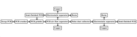
The PCB Recycling Process
The PCB recycling process involves several stages, each of which is crucial for the efficient recovery of valuable materials and the safe disposal of hazardous substances.
1. Collection and Sorting
The first step in the PCB recycling process is the collection and sorting of e-waste. Electronic devices are collected from various sources, such as households, businesses, and industrial facilities. The collected devices are then sorted based on their type, size, and material composition.
2. Dismantling and Separation
Once the devices are sorted, they are manually or mechanically dismantled to separate the PCBs from other components, such as plastic casings, cables, and batteries. The separated PCBs are then further categorized based on their size, type, and material content.
3. Shredding and Grinding
The separated PCBs are shredded and ground into smaller pieces using specialized equipment. This process helps to liberate the various materials present in the PCBs and prepares them for further processing.
4. Material Separation
The shredded PCB material undergoes a series of separation processes to recover the valuable materials. These processes may include:
a. Magnetic separation: Ferrous metals, such as iron and steel, are removed using powerful magnets.
b. Eddy current separation: Non-ferrous metals, like aluminum and copper, are separated using a rapidly alternating magnetic field.
c. Density separation: Plastics and other lightweight materials are separated from heavier metallic components using air or water-based density separation techniques.
5. Refining and Purification
The separated materials, particularly the precious metals, undergo further refining and purification processes to increase their purity and market value. This may involve chemical or electrochemical methods, such as leaching, electrowinning, or smelting.
6. Disposal of Hazardous Materials
The hazardous materials present in PCBs, such as lead and brominated flame retardants, are safely disposed of in accordance with local and international environmental regulations. These materials are typically treated, stabilized, and disposed of in secure landfills or through other approved methods to prevent environmental contamination.

Challenges in PCB Recycling
Despite the numerous benefits of PCB recycling, there are several challenges that the industry faces:
1. Complexity of PCB Composition
PCBs are complex in their composition, containing a wide range of materials, including metals, plastics, and ceramics. The varying concentrations and combinations of these materials make it challenging to develop efficient and cost-effective recycling processes.
2. Hazardous Material Management
The presence of hazardous materials in PCBs, such as lead and brominated flame retardants, poses significant health and environmental risks. Proper handling, storage, and disposal of these materials require strict adherence to safety regulations and substantial investments in specialized equipment and training.
3. Lack of Standardization
The absence of standardized designs and material compositions in PCBs makes it difficult to develop universal recycling processes. Different manufacturers use varying materials and construction methods, which complicates the recycling process and increases costs.
4. Insufficient Collection and Sorting Infrastructure
Effective PCB recycling relies on efficient collection and sorting systems. However, many regions lack the necessary infrastructure and awareness to ensure the proper collection and segregation of e-waste. This results in a significant portion of PCBs ending up in landfills or being exported to developing countries with inadequate recycling facilities.
5. Economic Viability
The economic viability of PCB recycling depends on several factors, such as the market prices of recovered materials, the cost of collection and processing, and the availability of government incentives. Fluctuations in market demand and the high initial investment required for setting up recycling facilities can impact the profitability of PCB recycling operations.

Best Practices in PCB Recycling
To overcome the challenges and ensure the success of PCB recycling, it is essential to adopt best practices throughout the recycling process:
1. Implement Effective Collection and Sorting Systems
Establish efficient collection and sorting systems to ensure the proper segregation of e-waste at the source. This can be achieved through public awareness campaigns, collaborations with local authorities and businesses, and the development of convenient collection points.
2. Invest in Advanced Recycling Technologies
Continuously invest in research and development to improve recycling technologies and processes. This includes developing more efficient separation techniques, automating certain stages of the recycling process, and finding innovative solutions for the recovery of valuable materials.
3. Adhere to Environmental and Safety Regulations
Strictly adhere to local and international environmental and safety regulations to minimize the risks associated with hazardous materials. Ensure that all employees are properly trained in handling e-waste and that the recycling facilities are equipped with the necessary safety equipment and pollution control systems.
4. Foster Collaborations and Partnerships
Encourage collaborations and partnerships among stakeholders, including manufacturers, recyclers, governments, and research institutions. These collaborations can help to develop standardized designs for PCBs, promote the use of eco-friendly materials, and establish efficient recycling networks.
5. Promote Circular Economy Principles
Embrace the principles of a circular economy by designing PCBs for easier recycling, encouraging the reuse of components, and promoting the use of recycled materials in the manufacturing of new products. This approach helps to minimize waste, conserve resources, and create a more sustainable electronics industry.
The Future of PCB Recycling
As the global demand for electronic devices continues to grow, the importance of PCB recycling will only increase in the coming years. To ensure a sustainable future for the electronics industry, it is crucial to continue investing in research and development, promoting best practices, and raising public awareness about the importance of e-waste recycling.
Some of the key trends and developments that are likely to shape the future of PCB recycling include:
- Increased automation and the use of artificial intelligence in recycling processes
- The development of more efficient and environmentally friendly recycling technologies
- Greater emphasis on eco-design and the use of recyclable materials in PCB manufacturing
- Stricter environmental regulations and increased government support for e-waste recycling initiatives
- Growing public awareness and participation in e-waste collection and recycling programs
By embracing these trends and working together towards a common goal, we can create a more sustainable and resilient electronics industry that minimizes its environmental impact and maximizes the value of its resources.
FAQs
1. What types of electronic devices contain PCBs?
PCBs are found in a wide range of electronic devices, including:
– Computers and laptops
– Smartphones and tablets
– Televisions and monitors
– Printers and scanners
– Home appliances (e.g., refrigerators, washing machines, and microwaves)
– Automotive electronics
– Industrial equipment and machinery
2. Can I recycle PCBs at home?
No, it is not recommended to attempt PCB recycling at home. The process requires specialized equipment, knowledge, and safety measures to handle the hazardous materials present in PCBs. It is best to dispose of e-waste containing PCBs through authorized recycling facilities or collection programs.
3. How can I find a reliable PCB recycling facility?
To find a reliable PCB recycling facility, you can:
– Check with your local government or environmental agency for information on authorized e-waste recyclers in your area
– Look for recyclers certified by e-Stewards or R2 (Responsible Recycling), which are internationally recognized standards for responsible e-waste recycling
– Contact the manufacturer of your electronic device for information on their recommended recycling programs or partners
4. Are there any health risks associated with handling PCBs?
Yes, handling PCBs without proper safety measures can pose health risks. PCBs contain hazardous materials, such as lead and brominated flame retardants, which can cause harm if inhaled, ingested, or absorbed through the skin. It is essential to wear appropriate personal protective equipment (PPE) and follow safe handling procedures when dealing with PCBs.
5. How can I support PCB recycling efforts in my community?
You can support PCB recycling efforts in your community by:
– Properly disposing of your e-waste through authorized recycling facilities or collection programs
– Spreading awareness about the importance of e-waste recycling among your family, friends, and colleagues
– Supporting businesses and organizations that prioritize responsible e-waste management and recycling practices
– Advocating for stronger e-waste recycling regulations and initiatives at the local and national levels
Conclusion
PCB recycling is a critical process that helps to mitigate the environmental impact of the growing e-waste problem while also recovering valuable materials for reuse in the manufacturing of new products. By understanding the importance of PCB recycling, the challenges it faces, and the best practices for implementing effective recycling systems, we can work towards creating a more sustainable and circular electronics industry.
As individuals, businesses, and governments, we all have a role to play in promoting responsible e-waste management and supporting PCB recycling efforts. By adopting eco-friendly practices, investing in advanced recycling technologies, and fostering collaborations among stakeholders, we can ensure a cleaner, healthier, and more resource-efficient future for generations to come.
| Material | Typical Content in PCBs | Environmental Impact | Health Risks |
|---|---|---|---|
| Copper | 20-30% | Resource depletion | Minimal |
| Gold | 0.1-0.2% | Resource depletion | Minimal |
| Silver | 0.2-0.3% | Resource depletion | Minimal |
| Palladium | 0.01-0.05% | Resource depletion | Minimal |
| Lead | 1-2% | Soil and water pollution | Neurological and developmental disorders |
| Brominated flame retardants | 1-5% | Persistent organic pollutants | Endocrine disruption and cancer |


Leave a Reply