Introduction to PCB Etching
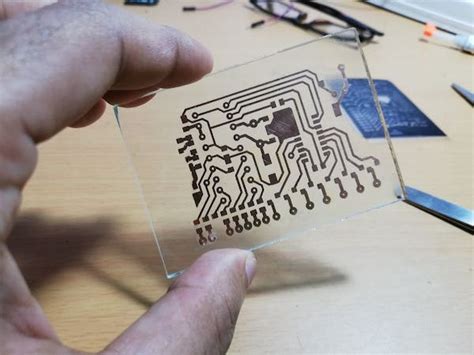
PCB etching is a crucial process in the fabrication of printed circuit boards (PCBs). It involves removing unwanted copper from the surface of a PCB substrate, leaving behind the desired conductive traces that form the electrical connections of the circuit. Achieving perfect PCB etching is essential for ensuring the reliability, functionality, and aesthetics of the final product.
In this comprehensive guide, we will explore the various techniques, materials, and best practices involved in PCB etching. Whether you are a hobbyist or a professional, this article will provide you with the knowledge and insights needed to achieve excellent results in your PCB etching endeavors.
Understanding the PCB Etching Process
PCB etching is a chemical process that selectively removes copper from the surface of a PCB substrate. The process begins with a PCB substrate that is coated with a thin layer of copper on one or both sides. The desired circuit pattern is then transferred onto the copper surface using a photoresist or a resist mask.
Once the resist pattern is in place, the PCB is immersed in an etching solution, which chemically reacts with the exposed copper areas. The etching solution dissolves the unwanted copper, leaving behind the protected copper traces that form the circuit pattern.
Types of PCB Etching
There are two main types of PCB etching: subtractive etching and additive etching.
-
Subtractive Etching: In subtractive etching, the PCB starts with a fully copper-clad substrate. The resist pattern is applied to protect the desired copper traces, and the unwanted copper is etched away. This is the most common method of PCB etching.
-
Additive Etching: Additive etching, also known as pattern plating, involves selectively adding copper to the PCB substrate. The resist pattern is applied to define the areas where copper should be deposited. Copper is then electroplated onto the exposed areas, forming the desired circuit traces.

PCB Etching Materials and Equipment
To achieve perfect PCB etching, it is essential to have the right materials and equipment. Here are the key components involved in the PCB etching process:
PCB Substrate
The PCB substrate is the base material on which the circuit is built. It is typically made of an insulating material, such as fiberglass or phenolic resin, with a thin layer of copper laminated on one or both sides. The choice of substrate depends on the specific requirements of the circuit, such as its size, thickness, and dielectric properties.
Photoresist
Photoresist is a light-sensitive material used to transfer the circuit pattern onto the copper surface of the PCB. It comes in two types: positive and negative.
- Positive Photoresist: When exposed to light, positive photoresist becomes soluble in the developer solution, allowing the exposed areas to be removed.
- Negative Photoresist: When exposed to light, negative photoresist becomes insoluble in the developer solution, allowing the unexposed areas to be removed.
Etching Solution
The etching solution is a chemical mixture used to dissolve the unwanted copper from the PCB surface. The most common etching solutions are:
- Ferric Chloride (FeCl3): Ferric chloride is a widely used etching solution known for its effectiveness and relatively low toxicity. It is available in liquid or powder form and can be reused multiple times.
- Ammonium Persulfate ((NH4)2S2O8): Ammonium persulfate is another popular etching solution that offers faster etching rates compared to ferric chloride. It is typically used in a heated bath to accelerate the etching process.
- Cupric Chloride (CuCl2): Cupric chloride is a less commonly used etching solution that provides a balance between etching speed and control. It is often used in regenerative etching systems.
Etching Equipment
To perform PCB etching, you will need the following equipment:
- Etching Tank: An etching tank is a container used to hold the etching solution and the PCB during the etching process. It should be made of a material that is resistant to the etching solution, such as plastic or glass.
- Heater: A heater is used to maintain the etching solution at the desired temperature, which typically ranges from 30°C to 50°C (86°F to 122°F). Higher temperatures accelerate the etching process but may reduce the control over the etching quality.
- Agitation System: An agitation system helps to ensure even etching by circulating the etching solution around the PCB. This can be achieved through manual agitation, air bubbling, or mechanical stirring.
- Ventilation: Proper ventilation is essential to remove the fumes generated during the etching process. A fume hood or an outdoor etching area with good airflow is recommended.

PCB Etching Techniques
There are several techniques used for PCB etching, each with its own advantages and considerations. Let’s explore the most common PCB etching techniques:
Immersion Etching
Immersion etching is the simplest and most straightforward PCB etching technique. It involves submerging the PCB in the etching solution and allowing the chemical reaction to take place. The etching process continues until all the unwanted copper is removed.
Advantages:
– Simple setup and process
– Suitable for small-scale production and hobbyist use
– Low cost
Considerations:
– Longer etching times compared to other techniques
– Requires manual agitation for even etching
– Limited control over the etching process
Spray Etching
Spray etching uses a pressurized spray of etching solution to remove the unwanted copper from the PCB surface. The PCB is placed in a spray etching machine, where the etching solution is sprayed onto the board from multiple angles.
Advantages:
– Faster etching times compared to immersion etching
– More even and consistent etching results
– Suitable for larger-scale production
Considerations:
– Higher equipment cost
– Requires specialized spray etching machines
– Increased safety considerations due to pressurized etching solution
Bubble Etching
Bubble etching involves immersing the PCB in the etching solution while introducing air bubbles to agitate the solution. The air bubbles help to circulate the etching solution and promote even etching.
Advantages:
– Improved etching uniformity compared to immersion etching
– Relatively simple setup
– Lower cost compared to spray etching
Considerations:
– Requires an air pump or compressed air source
– May produce uneven etching if air distribution is not optimized
– Increased noise level due to air bubbling
Regenerative Etching
Regenerative etching is an advanced technique that continuously regenerates the etching solution during the etching process. It involves circulating the etching solution through a regeneration system that removes the dissolved copper and replenishes the active ingredients.
Advantages:
– Consistent etching quality over time
– Reduced waste and disposal costs
– Longer etching solution life
Considerations:
– Higher initial equipment cost
– Requires specialized regenerative etching systems
– More complex setup and maintenance

Factors Affecting PCB Etching Quality
Several factors can influence the quality and consistency of PCB etching results. Understanding and controlling these factors is crucial for achieving perfect PCB etching.
Etching Solution Concentration
The concentration of the etching solution plays a significant role in the etching speed and quality. Higher concentrations generally result in faster etching rates but may reduce the control over the process. It is essential to follow the manufacturer’s recommendations for the optimal concentration range.
Etching Temperature
The temperature of the etching solution affects the etching rate and the quality of the results. Higher temperatures accelerate the etching process but may lead to over-etching or undercutting of the copper traces. Maintaining a consistent temperature throughout the etching process is crucial for achieving uniform results.
Agitation
Proper agitation of the etching solution ensures even distribution of the etchant and prevents the formation of localized etching hotspots. Inadequate agitation can result in uneven etching, with some areas being over-etched while others remain under-etched.
Etching Time
The etching time determines the amount of copper removed from the PCB surface. Insufficient etching time may leave unwanted copper residues, while excessive etching time can lead to over-etching and damage to the desired copper traces. It is important to monitor the etching progress and stop the process at the appropriate time.
Resist Quality
The quality and integrity of the resist pattern directly impact the accuracy and sharpness of the etched circuit traces. A high-quality resist with good adhesion and resolution is essential for achieving precise and well-defined etching results.
Best Practices for Perfect PCB Etching
To achieve the best possible PCB etching results, consider the following best practices:
-
Choose the right etching technique: Select the etching technique that best suits your needs based on factors such as production scale, desired etching speed, and available resources.
-
Maintain consistent etching conditions: Ensure that the etching solution concentration, temperature, and agitation are maintained within the optimal range throughout the etching process.
-
Monitor the etching progress: Regularly check the etching progress to avoid over-etching or under-etching. Use a timer and visual inspection to determine when to stop the etching process.
-
Use fresh etching solution: Replace the etching solution when it becomes saturated with dissolved copper or loses its effectiveness. Regular solution maintenance helps to maintain consistent etching quality.
-
Ensure proper ventilation: Perform PCB etching in a well-ventilated area or use a fume hood to remove harmful fumes generated during the process.
-
Follow safety precautions: Wear appropriate personal protective equipment (PPE) such as gloves, goggles, and an apron when handling etching solutions and working with PCBs.
-
Post-etching cleaning: After etching, thoroughly rinse the PCB with water to remove any residual etching solution. Use a mild abrasive or a dedicated PCB cleaner to remove the resist and expose the final circuit traces.
Troubleshooting Common PCB Etching Issues
Despite following best practices, you may encounter issues during the PCB etching process. Here are some common problems and their potential solutions:
-
Over-etching: If the copper traces appear thin or partially etched away, it indicates over-etching. To prevent this, reduce the etching time, lower the etching solution concentration, or decrease the etching temperature.
-
Under-etching: If unwanted copper remains on the PCB surface after etching, it suggests under-etching. Increase the etching time, raise the etching solution concentration, or ensure proper agitation to resolve this issue.
-
Uneven etching: Uneven etching can result in inconsistent copper removal across the PCB. Improve the agitation of the etching solution, ensure consistent temperature distribution, and verify the uniformity of the resist pattern.
-
Poor resist adhesion: If the resist pattern lifts or peels during etching, it indicates poor resist adhesion. Ensure proper surface cleaning before applying the resist, use a high-quality resist, and follow the recommended application and curing procedures.
-
Incomplete etching: Incomplete etching can occur if the etching solution becomes exhausted or if the etching time is insufficient. Replace the etching solution and increase the etching time as needed.
Environmental and Safety Considerations
PCB etching involves the use of chemicals that can be harmful to the environment and human health if not handled properly. It is crucial to prioritize safety and environmental responsibility during the etching process.
-
Proper disposal: Dispose of used etching solutions and rinse water in accordance with local regulations. Never pour them down the drain or into the environment without proper treatment.
-
Personal protective equipment (PPE): Always wear appropriate PPE, including gloves, goggles, and an apron, when handling etching solutions and working with PCBs.
-
Ventilation: Ensure adequate ventilation to remove harmful fumes generated during the etching process. Use a fume hood or perform etching in a well-ventilated area.
-
Storage and handling: Store etching solutions and chemicals in properly labeled containers and keep them away from heat, sparks, and open flames. Follow the manufacturer’s guidelines for safe handling and storage.
-
Spill response: Have a spill response plan in place and keep appropriate spill clean-up materials readily available in case of accidental spills or leaks.
Frequently Asked Questions (FAQ)
-
What is the best etching solution for PCB etching?
The choice of etching solution depends on factors such as etching speed, control, and availability. Ferric chloride (FeCl3) and ammonium persulfate ((NH4)2S2O8) are the most commonly used etching solutions. Ferric chloride is known for its effectiveness and relatively low toxicity, while ammonium persulfate offers faster etching rates. -
How long does PCB etching take?
The etching time varies depending on factors such as the etching solution concentration, temperature, and the desired amount of copper removal. Typically, the etching process can take anywhere from a few minutes to an hour. It is important to monitor the etching progress and stop the process at the appropriate time to avoid over-etching or under-etching. -
Can I reuse the etching solution?
Yes, etching solutions can be reused multiple times until they become saturated with dissolved copper or lose their effectiveness. However, it is important to monitor the solution’s performance and replace it when necessary to maintain consistent etching quality. -
How do I dispose of used etching solutions?
Used etching solutions should be disposed of in accordance with local regulations. Contact your local waste management authority for guidance on the proper disposal procedures in your area. Never pour used etching solutions down the drain or into the environment without proper treatment. -
What safety precautions should I take during PCB etching?
When performing PCB etching, it is crucial to prioritize safety. Always wear appropriate personal protective equipment (PPE) such as gloves, goggles, and an apron when handling etching solutions and working with PCBs. Ensure proper ventilation to remove harmful fumes, and follow the manufacturer’s guidelines for safe handling and storage of etching chemicals.
Conclusion
Achieving perfect PCB etching requires a combination of the right materials, techniques, and best practices. By understanding the PCB etching process, selecting the appropriate etching solution and equipment, and following the guidelines outlined in this article, you can produce high-quality PCBs with precise and reliable circuit traces.
Remember to prioritize safety and environmental responsibility throughout the etching process. Always handle etching chemicals with care, use appropriate personal protective equipment, and dispose of used solutions in accordance with local regulations.
With practice and attention to detail, you can master the art of PCB etching and bring your electronic projects to life with professionally etched circuit boards. Happy etching!
| Etching Technique | Advantages | Considerations |
|---|---|---|
| Immersion Etching | – Simple setup and process | – Longer etching times |
| – Suitable for small-scale production | – Requires manual agitation | |
| – Low cost | – Limited control over the etching process | |
| Spray Etching | – Faster etching times | – Higher equipment cost |
| – More even and consistent etching results | – Requires specialized spray etching machines | |
| – Suitable for larger-scale production | – Increased safety considerations | |
| Bubble Etching | – Improved etching uniformity | – Requires an air pump or compressed air source |
| – Relatively simple setup | – May produce uneven etching if air distribution is not optimized | |
| – Lower cost compared to spray etching | – Increased noise level due to air bubbling | |
| Regenerative Etching | – Consistent etching quality over time | – Higher initial equipment cost |
| – Reduced waste and disposal costs | – Requires specialized regenerative etching systems | |
| – Longer etching solution life | – More complex setup and maintenance |


Leave a Reply