Introduction to PCB Etching
Printed Circuit Board (PCB) etching is a crucial process in the manufacturing of electronic devices. It involves removing unwanted copper from the surface of the PCB to create the desired circuit pattern. The choice of etching method can significantly impact the quality, precision, and efficiency of the PCB fabrication process.
In this article, we will explore the two main types of PCB etching: wet etching and dry etching. We will discuss their principles, advantages, disadvantages, and applications to help you make an informed decision when selecting an etching solution for your PCB projects.
Wet Etching for PCB
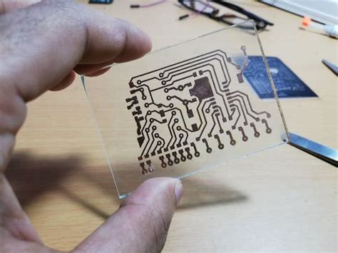
Wet etching, also known as chemical etching, is the most common method used in PCB fabrication. It involves using a chemical solution to dissolve the unwanted copper from the PCB surface, leaving behind the desired circuit pattern.
The Wet Etching Process
-
PCB Preparation: The PCB is cleaned and coated with a photoresist layer, which is then exposed to UV light through a photomask containing the circuit pattern.
-
Developing: The exposed photoresist is developed, revealing the copper areas to be etched.
-
Etching: The PCB is immersed in an etching solution, typically containing ferric chloride or ammonium persulfate. The solution reacts with the exposed copper, dissolving it and leaving behind the desired circuit traces.
-
Stripping: The remaining photoresist is removed using a stripping solution, revealing the final PCB with the etched circuit pattern.
Advantages of Wet Etching
- Low cost and simple setup
- Suitable for high-volume production
- Versatile and can handle complex circuit designs
- Relatively fast etching process
Disadvantages of Wet Etching
- Isotropic etching, resulting in undercuts and wider traces
- Disposal of hazardous chemical waste
- Limited resolution compared to dry etching methods
- Potential for over-etching or incomplete etching

Dry Etching for PCB
Dry etching, also known as plasma etching, is a more advanced method that uses a plasma to remove the unwanted copper from the PCB surface. It offers higher precision and resolution compared to wet etching.
The Dry Etching Process
-
PCB Preparation: Similar to wet etching, the PCB is cleaned and coated with a photoresist layer, which is then exposed to UV light through a photomask.
-
Developing: The exposed photoresist is developed, revealing the copper areas to be etched.
-
Plasma Etching: The PCB is placed in a vacuum chamber, and a plasma is generated using a high-frequency electric field. The plasma contains reactive ions that bombard the exposed copper, etching it away.
-
Stripping: The remaining photoresist is removed using a stripping solution or plasma ashing, revealing the final PCB with the etched circuit pattern.
Advantages of Dry Etching
- Anisotropic etching, resulting in precise and uniform trace widths
- Higher resolution and finer pitch capabilities
- No hazardous chemical waste
- Suitable for high-density and multilayer PCBs
Disadvantages of Dry Etching
- Higher equipment and operating costs
- Slower etching process compared to wet etching
- Requires specialized knowledge and skilled operators
- Limited substrate compatibility

Comparison of Wet and Dry Etching
| Parameter | Wet Etching | Dry Etching |
|---|---|---|
| Etching Mechanism | Chemical dissolution | Plasma bombardment |
| Etching Profile | Isotropic (undercuts) | Anisotropic (straight walls) |
| Resolution | Limited (>100 μm) | High (<1 μm) |
| Etching Speed | Fast (1-10 μm/min) | Slow (0.1-1 μm/min) |
| Chemical Waste | Hazardous liquid waste | Minimal or no liquid waste |
| Equipment Cost | Low | High |
| Operating Cost | Low | High |
| Skill Requirement | Moderate | High |
| Suitable Applications | High-volume, simple designs | High-density, complex designs |

Choosing the Right Etching Solution
When deciding between wet and dry etching for your PCB project, consider the following factors:
-
Circuit Complexity: For simple, low-density designs, wet etching is often sufficient. However, for high-density, multilayer, or fine-pitch designs, dry etching is the preferred choice.
-
Production Volume: Wet etching is more suitable for high-volume production due to its lower cost and faster etching speed. Dry etching is better suited for low-to-medium volume production or prototyping.
-
Resolution and Precision: If your application demands high resolution and precise trace widths, dry etching is the way to go. Wet etching has limitations in terms of resolution and can result in undercuts.
-
Budget and Resources: Wet etching has a lower initial investment and operating cost compared to dry etching. However, if your budget allows and you require the benefits of dry etching, it may be worth the investment.
-
Environmental Considerations: Wet etching generates hazardous chemical waste that requires proper disposal. Dry etching, on the other hand, produces minimal or no liquid waste, making it a more environmentally friendly option.
Frequently Asked Questions (FAQ)
-
Q: Can I use a combination of wet and dry etching for my PCB?
A: Yes, it is possible to use a combination of wet and dry etching techniques in a single PCB fabrication process. This is known as a hybrid etching approach, where wet etching is used for the majority of the copper removal, and dry etching is used for fine-tuning or creating specific features. -
Q: What is the typical resolution achievable with wet etching?
A: Wet etching typically achieves a resolution of around 100 μm or greater. The resolution is limited by factors such as the isotropic nature of the etching process, which can result in undercuts and wider traces. -
Q: How does the etching time compare between wet and dry etching?
A: Wet etching is generally faster than dry etching. The etching speed for wet etching ranges from 1 to 10 μm/min, while dry etching has a slower etching speed of 0.1 to 1 μm/min. However, the actual etching time depends on various factors, such as the copper thickness, etchant concentration, and temperature. -
Q: Are there any safety concerns associated with wet etching?
A: Yes, wet etching involves the use of hazardous chemicals, such as ferric chloride or ammonium persulfate. These chemicals can cause skin and eye irritation, and their fumes can be harmful if inhaled. Proper safety precautions, including personal protective equipment (PPE) and adequate ventilation, must be in place when working with wet etching solutions. -
Q: What are the common materials used for dry etching in PCB fabrication?
A: The most common materials used for dry etching in PCB fabrication are chlorine-based gases, such as chlorine (Cl2) and boron trichloride (BCl3). These gases are highly reactive and form volatile compounds with copper, enabling the etching process. Other gases, such as argon (Ar) and nitrogen (N2), are used for plasma generation and process control.
Conclusion
Choosing the right etching solution for your PCB project is crucial for achieving the desired circuit quality, precision, and efficiency. Wet etching offers a low-cost and simple solution for high-volume production and complex designs, while dry etching provides higher resolution and precision for high-density and multilayer PCBs.
By understanding the principles, advantages, and disadvantages of each etching method, you can make an informed decision based on your specific project requirements, budget, and environmental considerations. Whether you opt for wet etching, dry etching, or a hybrid approach, selecting the appropriate etching solution will help you create reliable and high-quality PCBs for your electronic devices.


Leave a Reply