Introduction to PCB Development and Emerging Trends
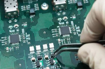
Printed Circuit Boards (PCBs) are the backbone of modern electronics. These thin boards made of fiberglass or composite material provide mechanical support and electrical connections for electronic components using conductive pathways, tracks, or signal traces etched from copper sheets. PCBs have revolutionized the electronics industry by enabling the production of smaller, cheaper, and more reliable electronic devices.
As technology continues to advance at a rapid pace, the PCB industry must keep up with the latest trends and innovations. In this article, we will explore the future trends in PCB development that are shaping the industry and driving innovation.
Trend 1: Miniaturization and High-Density Interconnect (HDI) PCBs
One of the most significant trends in PCB development is miniaturization. As electronic devices become smaller and more compact, PCBs must also shrink in size while maintaining their functionality. High-Density Interconnect (HDI) PCBs are a solution to this challenge.
HDI PCBs feature finer lines and spaces, smaller vias, and higher connection pad density than traditional PCBs. This allows for more components to be placed in a smaller area, enabling the production of smaller and more powerful electronic devices.
| Feature | Traditional PCB | HDI PCB |
|---|---|---|
| Line width/space | >100µm | <100µm |
| Via diameter | >150µm | <150µm |
| Connection pad density | Low | High |
The demand for HDI PCBs is growing rapidly, driven by the increasing miniaturization of electronic devices. According to a report by Global Market Insights, the HDI PCB market size is expected to exceed USD 22 billion by 2024, growing at a CAGR of over 11% from 2018 to 2024.
Applications of HDI PCBs
HDI PCBs are used in a wide range of applications, including:
- Smartphones and tablets
- Wearable devices
- Medical devices
- Automotive electronics
- Aerospace and defense systems

Trend 2: Flexible and Stretchable PCBs
Another trend in PCB development is the use of flexible and stretchable materials. Traditional PCBs are rigid and cannot be bent or stretched without damaging the board. However, the growing demand for wearable devices and flexible electronics has led to the development of flexible and stretchable PCBs.
Flexible PCBs are made from thin, flexible materials such as polyimide or polyester. They can be bent and folded without damaging the board or the components. Stretchable PCBs, on the other hand, can be stretched and deformed without losing their electrical conductivity. They are made from elastic materials such as silicone or polyurethane.
| PCB Type | Material | Flexibility | Stretchability |
|---|---|---|---|
| Rigid PCB | FR-4 | None | None |
| Flexible PCB | Polyimide, Polyester | High | None |
| Stretchable PCB | Silicone, Polyurethane | High | High |
Flexible and stretchable PCBs have numerous applications, including:
- Wearable devices such as smartwatches and fitness trackers
- Medical devices such as implantable sensors and prosthetics
- Automotive electronics such as sensors and displays
- Aerospace and defense systems such as radar and communication devices

Trend 3: 3D Printing of PCBs
3D printing is a rapidly growing technology that has the potential to revolutionize the PCB industry. Traditional PCB manufacturing involves multiple steps, including designing the board, creating a photomask, etching the copper, and drilling holes. This process is time-consuming and requires specialized equipment.
3D printing, on the other hand, allows for the rapid prototyping and production of PCBs without the need for specialized equipment. PCBs can be printed using conductive inks or filaments, allowing for the creation of complex shapes and structures that are not possible with traditional manufacturing methods.
| Feature | Traditional PCB Manufacturing | 3D Printed PCBs |
|---|---|---|
| Time | Slow | Fast |
| Cost | High | Low |
| Complexity | Limited | High |
| Customization | Limited | High |
3D printing of PCBs has numerous advantages, including:
- Rapid prototyping and iteration
- Reduced costs and lead times
- Increased design flexibility and customization
- Ability to create complex shapes and structures
Applications of 3D Printed PCBs
3D printed PCBs have numerous potential applications, including:
- Rapid prototyping and testing of new designs
- Low-volume production runs
- Customized and personalized electronics
- Aerospace and defense systems
- Medical devices and implants

Trend 4: Eco-Friendly and Sustainable PCBs
As concerns about the environment and sustainability continue to grow, there is a growing demand for eco-friendly and sustainable PCBs. Traditional PCB manufacturing involves the use of hazardous chemicals and materials, such as lead and halogenated flame retardants, which can have negative impacts on the environment and human health.
Eco-friendly and sustainable PCBs are made from materials that are biodegradable, recyclable, or renewable. They also use manufacturing processes that minimize waste and reduce the use of hazardous chemicals.
| Material | Traditional PCB | Eco-Friendly PCB |
|---|---|---|
| Substrate | FR-4 | Biodegradable materials (e.g. cellulose, PLA) |
| Solder | Lead-based | Lead-free |
| Flame retardants | Halogenated | Halogen-free |
Eco-friendly and sustainable PCBs have numerous benefits, including:
- Reduced environmental impact
- Improved human health and safety
- Compliance with environmental regulations and standards
- Improved brand reputation and customer perception
Applications of Eco-Friendly and Sustainable PCBs
Eco-friendly and sustainable PCBs are being used in a growing number of applications, including:
- Consumer electronics
- Automotive electronics
- Medical devices
- Aerospace and defense systems
- Industrial automation and control systems
Trend 5: Artificial Intelligence and Machine Learning in PCB Development
Artificial Intelligence (AI) and Machine Learning (ML) are transforming many industries, and the PCB industry is no exception. AI and ML can be used to optimize PCB design, manufacturing, and testing processes, leading to faster development times, lower costs, and improved quality.
Some of the applications of AI and ML in PCB development include:
- Automated PCB design and layout optimization
- Predictive maintenance and quality control
- Supply chain optimization and demand forecasting
- Automated visual inspection and defect detection
| Process | Traditional Method | AI/ML Method |
|---|---|---|
| PCB design | Manual, time-consuming | Automated, optimized |
| Quality control | Manual inspection | Automated visual inspection |
| Supply chain | Manual forecasting | Predictive analytics |
The use of AI and ML in PCB development is still in its early stages, but it has the potential to revolutionize the industry and drive significant improvements in efficiency, quality, and cost.
FAQ
Q1: What is a High-Density Interconnect (HDI) PCB?
A1: A High-Density Interconnect (HDI) PCB is a type of PCB that features finer lines and spaces, smaller vias, and higher connection pad density than traditional PCBs. This allows for more components to be placed in a smaller area, enabling the production of smaller and more powerful electronic devices.
Q2: What are the benefits of using flexible and stretchable PCBs?
A2: Flexible and stretchable PCBs offer several benefits over traditional rigid PCBs. They can be bent, folded, and stretched without damaging the board or components, making them ideal for use in wearable devices, medical implants, and other applications where flexibility and stretchability are important. They also enable the creation of new form factors and designs that are not possible with rigid PCBs.
Q3: How does 3D printing of PCBs work?
A3: 3D printing of PCBs involves using conductive inks or filaments to print the conductive traces and components directly onto a substrate material. The process typically involves multiple layers of conductive and insulating materials, which are built up layer by layer to create the final PCB. 3D printing allows for rapid prototyping and production of PCBs without the need for specialized equipment or tooling.
Q4: What are the benefits of using eco-friendly and sustainable PCBs?
A4: Eco-friendly and sustainable PCBs offer several benefits over traditional PCBs. They are made from materials that are biodegradable, recyclable, or renewable, and use manufacturing processes that minimize waste and reduce the use of hazardous chemicals. This reduces the environmental impact of PCB production and disposal, and can improve human health and safety. Eco-friendly and sustainable PCBs can also help companies comply with environmental regulations and standards, and improve their brand reputation and customer perception.
Q5: What are some of the applications of AI and ML in PCB development?
A5: AI and ML can be used in several aspects of PCB development, including automated PCB design and layout optimization, predictive maintenance and quality control, supply chain optimization and demand forecasting, and automated visual inspection and defect detection. These applications can help reduce development times, lower costs, and improve the quality and reliability of PCBs.
Conclusion
The PCB industry is constantly evolving, driven by advances in technology and changing market demands. The future trends in PCB development, including miniaturization and HDI PCBs, flexible and stretchable PCBs, 3D printing of PCBs, eco-friendly and sustainable PCBs, and the use of AI and ML in PCB development, are shaping the industry and driving innovation.
As these trends continue to evolve and mature, we can expect to see significant improvements in the performance, reliability, and sustainability of PCBs, as well as the development of new applications and use cases. Companies that are able to stay ahead of these trends and adapt to the changing market will be well-positioned for success in the years to come.


Leave a Reply