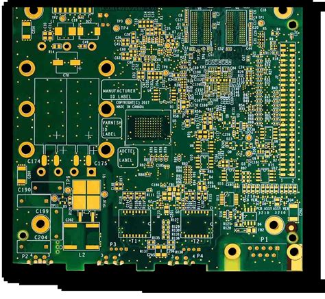
Introduction to HDI PCBs
High Density Interconnect (HDI) Printed Circuit Boards (PCBs) are a type of circuit board that offers higher wiring density than traditional PCBs. HDI PCBs have finer lines and spaces (<100 μm), smaller vias (<150 μm), and capture pads (<400 μm), and higher connection pad density (>20 pads/cm²) compared to conventional PCBs.
HDI technology enables the design of compact, lightweight electronic products with enhanced functionality and performance. These boards are widely used in smartphones, tablets, laptops, wearable devices, medical equipment, aerospace systems, and military applications.
Advantages of HDI PCBs
HDI PCBs offer several benefits over traditional PCBs:
-
Miniaturization: HDI technology allows for smaller component sizes and higher density interconnects, enabling the design of compact and lightweight electronic devices.
-
Improved Signal Integrity: Shorter signal paths and reduced layer count in HDI PCBs minimize signal loss, crosstalk, and electromagnetic interference (EMI), resulting in improved signal integrity.
-
Enhanced Reliability: HDI PCBs have smaller vias and thinner dielectric layers, which reduce thermal stress and improve the reliability of the board.
-
Increased Functionality: With higher interconnect density, HDI PCBs can accommodate more components and functions in a smaller area, enabling the design of feature-rich electronic products.
-
Cost-Effective: Although the initial cost of HDI PCBs may be higher than traditional PCBs, they offer cost savings in terms of reduced board size, layer count, and assembly complexity.

HDI PCB Design Considerations
When designing HDI PCBs, several factors must be considered to ensure optimal performance, reliability, and manufacturability:
1. Material Selection
The choice of PCB material is crucial in HDI design. The material should have good thermal, mechanical, and electrical properties to withstand the high-density interconnect requirements. Some common materials used in HDI PCBs include:
| Material | Dielectric Constant | Dissipation Factor | Thermal Conductivity (W/mK) | Tg (°C) |
|---|---|---|---|---|
| FR-4 | 4.2 – 4.5 | 0.02 | 0.3 | 130-140 |
| Polyimide | 3.2 – 3.5 | 0.002 – 0.003 | 0.2 | 250-260 |
| Rogers 4350B | 3.48 | 0.004 | 0.62 | >280 |
| Isola I-Speed | 2.6 – 2.8 | 0.003 – 0.006 | 0.25 | 140-180 |
2. Layer Stack-up
The layer stack-up of an HDI PCB plays a vital role in signal integrity, EMI performance, and manufacturability. A typical HDI PCB stack-up may include:
- Core layers: Thicker dielectric layers that provide mechanical support and allow for through-hole vias.
- Microvias: Small, laser-drilled vias that connect the outer layers to the inner layers.
- Buried vias: Vias that connect inner layers without reaching the outer layers.
- Blind vias: Vias that start from an outer layer and terminate at an inner layer.
An example of a 6-layer HDI PCB stack-up:
| Layer | Material | Thickness (μm) |
|---|---|---|
| Top | Copper | 18 |
| Prepreg | FR-4 | 100 |
| Inner 1 | Copper | 35 |
| Core | FR-4 | 200 |
| Inner 2 | Copper | 35 |
| Prepreg | FR-4 | 100 |
| Bottom | Copper | 18 |
3. Via Types and Sizes
HDI PCBs employ various types of vias with smaller sizes compared to traditional PCBs. The choice of via type and size depends on the design requirements, layer count, and manufacturing capabilities. Some common via types used in HDI PCBs are:
| Via Type | Diameter (μm) | Drill Size (μm) | Aspect Ratio |
|---|---|---|---|
| Through | 200 – 300 | 150 – 200 | 8:1 – 10:1 |
| Blind | 100 – 200 | 50 – 150 | 1:1 – 1:1.2 |
| Buried | 100 – 200 | 50 – 150 | 1:1 – 1:1.2 |
| Microvia | 50 – 150 | 25 – 100 | 1:1 – 1:1.2 |
4. Trace Width and Spacing
HDI PCBs have finer trace widths and spacing compared to traditional PCBs, enabling higher wiring density. The minimum trace width and spacing depend on the PCB material, copper thickness, and manufacturing process. Typical values for HDI PCBs are:
| Copper Thickness (μm) | Minimum Trace Width (μm) | Minimum Spacing (μm) |
|---|---|---|
| 18 | 75 | 75 |
| 35 | 100 | 100 |
| 70 | 120 | 120 |
5. Component Placement and Routing
Proper component placement and routing are essential for optimal signal integrity, thermal management, and manufacturability in HDI PCBs. Some guidelines to follow:
- Place components close to their associated circuitry to minimize signal path lengths.
- Avoid routing traces over split planes or gaps in the reference plane to minimize impedance discontinuities.
- Use via-in-pad or blind vias for component connections to reduce board size and improve routing density.
- Follow the manufacturer’s recommended land pattern and clearance requirements for components.
- Route critical signals on inner layers sandwiched between ground planes to minimize crosstalk and EMI.

HDI PCB Manufacturing Process
The manufacturing process for HDI PCBs is more complex than traditional PCBs due to the smaller features and higher density interconnects. The process typically involves the following steps:
-
Material Preparation: The PCB material is cut to size, cleaned, and copper-clad if necessary.
-
Drilling: Through-holes, blind vias, and buried vias are drilled using mechanical or laser drilling processes.
-
Plating: The drilled holes are plated with copper to create electrical connections between layers.
-
Patterning: The outer layer copper is patterned using photolithography and etching processes to create traces, pads, and planes.
-
Lamination: The patterned layers are stacked and laminated together under high pressure and temperature to form a solid board.
-
Solder Mask and Silkscreen: A solder mask is applied to protect the copper traces, and a silkscreen is added for component labeling and identification.
-
Surface Finish: A surface finish, such as HASL, ENIG, or OSP, is applied to protect the exposed copper and improve solderability.
-
Electrical Testing: The completed PCB undergoes electrical testing to ensure proper functionality and connectivity.

HDI PCB Design Software
Several PCB design software packages support HDI design features and constraints. Some popular options include:
- Altium Designer
- Cadence Allegro
- Mentor Graphics PADS
- OrCAD PCB Designer
- Zuken CR-8000
These software tools offer advanced features such as via-in-pad support, microvias, embedded components, and design rule checking (DRC) for HDI constraints.
HDI PCB Design Guidelines
To ensure successful HDI PCB design and manufacturing, follow these guidelines:
-
Collaborate with the manufacturer: Engage with the PCB manufacturer early in the design process to discuss design requirements, manufacturing capabilities, and cost targets.
-
Follow HDI design rules: Adhere to the manufacturer’s HDI design rules for minimum trace width, spacing, via sizes, and clearances to ensure manufacturability and reliability.
-
Optimize layer stack-up: Choose the appropriate layer stack-up and material to meet the signal integrity, thermal, and mechanical requirements of the design.
-
Minimize via count: Use blind, buried, and microvias judiciously to minimize the overall via count and improve routing density.
-
Avoid stubs: Minimize the use of via stubs, which can cause signal reflections and degrade signal integrity. Use blind vias or back-drilling to remove stubs.
-
Optimize power distribution: Use separate power planes for different voltage levels and avoid splitting planes unnecessarily. Use decoupling capacitors close to power pins to minimize noise.
-
Simulate and validate: Perform signal integrity simulations and design rule checks to validate the HDI PCB design before manufacturing.
FAQ
-
Q: What is the minimum feature size for HDI PCBs?
A: The minimum feature size for HDI PCBs depends on the manufacturer’s capabilities. Typically, HDI PCBs have trace widths and spacing < 100 μm, microvias < 150 μm, and capture pads < 400 μm. -
Q: How many layers can an HDI PCB have?
A: HDI PCBs can have up to 24 layers or more, depending on the design requirements and manufacturing capabilities. However, most HDI designs have 6 to 12 layers. -
Q: What is the cost difference between HDI and traditional PCBs?
A: HDI PCBs are generally more expensive than traditional PCBs due to the complex manufacturing process and advanced materials used. However, HDI PCBs can offer cost savings in terms of reduced board size, layer count, and assembly complexity. -
Q: Can HDI PCBs be used for high-power applications?
A: HDI PCBs can be used for high-power applications, but special considerations must be made for thermal management, current carrying capacity, and voltage isolation. The use of thicker copper, thermal vias, and appropriate material selection can help mitigate these challenges. -
Q: What are the challenges in HDI PCB assembly?
A: HDI PCB assembly can be challenging due to the smaller component sizes, finer pitch, and higher density interconnects. Challenges include component placement accuracy, soldering quality, and inspection. Advanced assembly processes such as surface mount technology (SMT), chip-scale packaging (CSP), and ball grid array (BGA) are often used for HDI PCB assembly.
Conclusion
HDI PCB design offers numerous benefits for modern electronic products, including miniaturization, improved signal integrity, enhanced reliability, increased functionality, and cost-effectiveness. However, designing HDI PCBs requires careful consideration of materials, layer stack-up, via types and sizes, trace widths and spacing, component placement, and routing.
By following HDI design guidelines, collaborating with manufacturers, and using advanced PCB design software, engineers can create HDI PCBs that are optimized for performance, reliability, and manufacturability. As electronic devices continue to shrink in size and increase in complexity, HDI technology will play an increasingly important role in enabling the next generation of innovative products.


Leave a Reply