What is a PCB?
A Printed Circuit Board, or PCB, is a thin board made of fiberglass or composite material that is used to mechanically support and electrically connect electronic components using conductive pathways, tracks, or signal traces etched from copper sheets laminated onto a non-conductive substrate. PCBs are the foundation of almost all electronic devices we use today, from smartphones and computers to medical equipment and aerospace systems.
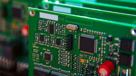
Key Features of PCBs
- Non-conductive substrate: The base material of a PCB, typically made of fiberglass, epoxy, or composite materials.
- Copper layers: Thin sheets of copper laminated onto the substrate, which are etched to create conductive pathways.
- Solder mask: A protective layer applied over the copper traces to prevent short circuits and provide insulation.
- Silkscreen: Text, symbols, and logos printed on the PCB for identification and assembly purposes.
- Vias: Holes drilled through the PCB to connect different layers of copper.
- Components: Electronic parts such as resistors, capacitors, and integrated circuits that are soldered onto the PCB.
Types of PCBs
There are several types of PCBs, each with its own unique features and applications:
Single-Layer PCBs
Single-layer PCBs, also known as single-sided PCBs, have conductive traces on only one side of the substrate. These boards are the simplest and most cost-effective type of PCB, making them ideal for low-complexity circuits and hobbyist projects.
Double-Layer PCBs
Double-layer PCBs have conductive traces on both sides of the substrate, allowing for more complex circuits and higher component density compared to single-layer boards. The two layers are connected using vias, which are holes drilled through the board and plated with conductive material.
Multi-Layer PCBs
Multi-layer PCBs consist of three or more layers of conductive traces separated by insulating layers. These boards offer the highest level of complexity and component density, making them suitable for advanced applications such as high-speed digital circuits, smartphones, and medical devices.
| PCB Type | Layers | Complexity | Cost | Applications |
|---|---|---|---|---|
| Single-Layer | 1 | Low | Low | Simple circuits, hobbyist projects |
| Double-Layer | 2 | Medium | Medium | More complex circuits, general electronics |
| Multi-Layer | 3+ | High | High | Advanced applications, high-speed digital circuits |
Flexible PCBs
Flexible PCBs, or flex PCBs, are made using a flexible substrate material such as polyimide or PEEK. These boards can bend and conform to various shapes, making them ideal for applications where space is limited or where the PCB needs to fit into a specific form factor.
Rigid-flex PCBs
Rigid-flex PCBs combine the benefits of both rigid and flexible PCBs by incorporating both types of substrates into a single board. The rigid sections provide structural support and house most of the components, while the flexible sections allow the board to bend and fit into tight spaces.

PCB Design Process
The PCB design process involves several steps, from concept to final production:
- Schematic design: Create a schematic diagram that represents the electrical connections between components.
- Component selection: Choose the appropriate components based on the circuit requirements and design constraints.
- PCB layout: Arrange the components and route the conductive traces on the board using PCB design software.
- Design rule check (DRC): Verify that the PCB layout meets the manufacturing and electrical requirements.
- Prototyping: Fabricate a prototype PCB to test and validate the design.
- Manufacturing: Once the design is finalized, the PCB is mass-produced using various manufacturing techniques.
PCB Design Software
There are several PCB design software packages available, ranging from free, open-source tools to professional-grade suites:
| Software | Vendor | Type | Price |
|---|---|---|---|
| KiCad | KiCad EDA | Open-source | Free |
| EAGLE | Autodesk | Commercial | Subscription-based |
| Altium Designer | Altium | Commercial | High-end |
| OrCAD | Cadence | Commercial | High-end |

PCB Manufacturing Techniques
PCBs are manufactured using various techniques, depending on the complexity, volume, and specific requirements of the board:
Etching
Etching is the process of removing unwanted copper from the substrate to create the desired conductive patterns. There are two main methods of etching:
- Chemical etching: The PCB is coated with a photoresist layer, which is then exposed to UV light through a photomask. The unexposed areas are dissolved using a chemical solution, leaving behind the desired copper traces.
- Mechanical etching: The copper is removed using a CNC machine or a laser, which selectively removes the unwanted copper based on the PCB design files.
Drilling
Drilling is the process of creating holes in the PCB for vias, component leads, and mounting purposes. This is typically done using a CNC drilling machine or a laser drill, which can create holes with high precision and accuracy.
Plating
Plating involves coating the drilled holes and exposed copper traces with a thin layer of conductive material, such as copper, silver, or gold. This process ensures reliable electrical connections and protects the copper from oxidation and corrosion.
Solder Mask and Silkscreen Application
The solder mask and silkscreen layers are applied to the PCB using a screen printing process or a photoimaging technique. The solder mask provides insulation and protection for the copper traces, while the silkscreen adds text, symbols, and logos for identification and assembly purposes.

PCB Assembly
Once the PCB is manufactured, the electronic components are assembled onto the board using various techniques:
Through-Hole Assembly
Through-hole components have long leads that are inserted into holes drilled through the PCB and soldered onto the opposite side. This method is suitable for larger components and provides a strong mechanical connection.
Surface-Mount Assembly
Surface-mount components are smaller and have flat leads or pads that are soldered directly onto the surface of the PCB. This method allows for higher component density and faster assembly compared to through-hole assembly.
Wave Soldering
Wave soldering is a process where the assembled PCB is passed over a wave of molten solder, which selectively coats the component leads and pads. This method is suitable for through-hole components and some surface-mount components.
Reflow Soldering
Reflow soldering involves applying solder paste to the PCB pads, placing the surface-mount components, and then heating the entire board in a reflow oven. The heat melts the solder paste, creating a permanent connection between the components and the PCB.
PCB Testing and Inspection
After assembly, PCBs undergo various testing and inspection processes to ensure quality and functionality:
Visual Inspection
A visual inspection is performed to check for any obvious defects, such as missing components, incorrect component placement, or solder bridges.
Automated Optical Inspection (AOI)
AOI uses cameras and image processing software to automatically detect assembly defects, such as missing or misaligned components, solder bridging, or insufficient solder joints.
X-Ray Inspection
X-ray inspection is used to examine the internal structure of the PCB, such as the quality of vias, the integrity of ball grid array (BGA) connections, and the presence of voids in solder joints.
Functional Testing
Functional testing involves powering up the PCB and verifying that it performs as intended, based on the design specifications and requirements.
PCB Applications
PCBs are used in a wide range of industries and applications, including:
- Consumer electronics: Smartphones, tablets, laptops, televisions, and home appliances.
- Automotive: Engine control units, infotainment systems, and advanced driver assistance systems (ADAS).
- Medical devices: Diagnostic equipment, monitoring systems, and implantable devices.
- Aerospace and defense: Avionics, communication systems, and military equipment.
- Industrial automation: Programmable logic controllers (PLCs), sensors, and control systems.
Frequently Asked Questions (FAQ)
1. What is the difference between a PCB and a breadboard?
A breadboard is a temporary prototyping tool used to build and test electronic circuits without soldering. PCBs, on the other hand, are permanent boards that mechanically support and electrically connect electronic components using conductive traces and solder.
2. Can I design my own PCB?
Yes, you can design your own PCB using various PCB design software packages, such as KiCad, EAGLE, or Altium Designer. However, designing a PCB requires knowledge of electronic circuits, PCB layout principles, and design rules.
3. How much does it cost to manufacture a PCB?
The cost of manufacturing a PCB depends on several factors, such as the board size, complexity, layer count, and quantity. For small quantities (1-10 boards), the cost can range from $10 to $100 per board, while larger quantities can benefit from economies of scale and cost less per board.
4. What is the typical turnaround time for PCB manufacturing?
The turnaround time for PCB manufacturing depends on the complexity of the board, the manufacturing process, and the supplier. For standard PCBs, the turnaround time can range from 1-2 weeks for small quantities to 4-6 weeks for larger orders. Some suppliers offer expedited services for faster turnaround times.
5. How do I choose the right PCB manufacturer?
When choosing a PCB manufacturer, consider factors such as their experience, capabilities, quality control processes, and customer support. Look for manufacturers with good reviews, competitive pricing, and a track record of delivering high-quality PCBs on time. It’s also essential to ensure that the manufacturer can meet your specific requirements, such as board complexity, material selection, and certifications (e.g., ISO, UL, or RoHS).
In conclusion, PCBs are the backbone of modern electronics, providing a reliable and efficient means of interconnecting electronic components. Understanding the basics of PCB design, manufacturing, and assembly is crucial for anyone involved in the development or production of electronic devices. As technology continues to advance, the importance of PCBs will only grow, driving innovation across various industries and shaping the future of electronics.


Leave a Reply