Introduction to PCB Boards
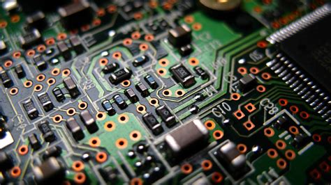
A printed circuit board (PCB) is a fundamental component in modern electronics. It is a flat board made of insulating materials, such as fiberglass or composite epoxy, with conductive pathways etched or printed onto its surface. These pathways, also known as traces, connect various electronic components, such as resistors, capacitors, and integrated circuits, to create a functional electronic device.
PCBs have revolutionized the electronics industry by providing a reliable, compact, and cost-effective means of assembling electronic circuits. They are used in a wide range of applications, from simple consumer electronics to complex industrial equipment and aerospace systems.
Types of PCB Boards
There are several types of PCB boards, each with its own unique characteristics and applications:
-
Single-sided PCB: These boards have conductive traces on only one side of the insulating substrate. They are the simplest and most cost-effective type of PCB, suitable for low-complexity circuits.
-
Double-sided PCB: These boards have conductive traces on both sides of the insulating substrate, allowing for more complex circuits and higher component density. The two sides are connected using through-hole technology.
-
Multi-layer PCB: These boards consist of multiple layers of insulating substrate with conductive traces on each layer. They offer the highest level of complexity and component density, making them suitable for advanced electronic applications.
-
Flexible PCB: These boards are made of flexible insulating materials, such as polyimide, allowing them to bend and conform to various shapes. They are commonly used in wearable electronics and applications where space is limited.
-
Rigid-flex PCB: These boards combine the features of rigid and flexible PCBs, with rigid sections for mounting components and flexible sections for connecting them. They offer the benefits of both types of PCBs in a single board.
PCB Board Materials
The choice of materials for a PCB board is crucial, as it affects the board’s performance, reliability, and cost. The most common materials used in PCB fabrication are:
Substrate Materials
-
FR-4: A composite material made of woven fiberglass cloth with an epoxy resin binder. It is the most widely used substrate material for PCBs due to its excellent mechanical and electrical properties, as well as its affordability.
-
High Tg FR-4: A variant of FR-4 with a higher glass transition temperature (Tg), offering better thermal stability and performance in high-temperature applications.
-
Polyimide: A high-performance polymer with excellent thermal and chemical resistance, making it suitable for flexible PCBs and applications with demanding environmental conditions.
-
Ceramic: A substrate material with excellent thermal conductivity and low dielectric constant, making it suitable for high-frequency and high-power applications.
Conductive Materials
-
Copper: The most common conductive material used in PCBs due to its excellent electrical conductivity, thermal conductivity, and affordability. Copper foils are laminated onto the substrate material and etched to create the desired conductive patterns.
-
Gold: A highly conductive and corrosion-resistant material used for plating contacts and connectors in high-reliability applications.
-
Silver: A highly conductive material used for special applications, such as RFID antennas and high-frequency circuits.
-
Aluminum: A lightweight and cost-effective alternative to copper, used in some high-power and high-frequency applications.

PCB Board Design Considerations
Designing a PCB board requires careful consideration of various factors to ensure optimal performance, reliability, and manufacturability. Some key design considerations include:
Component Placement
- Place components in a logical and organized manner, minimizing the distance between related components to reduce signal interference and power loss.
- Consider the mechanical constraints of the enclosure and the accessibility of components for assembly and maintenance.
Trace Routing
- Follow good routing practices, such as avoiding sharp angles, maintaining consistent trace width, and minimizing trace length to reduce signal integrity issues.
- Ensure proper spacing between traces to minimize crosstalk and electromagnetic interference (EMI).
Power and Ground Planes
- Use dedicated power and ground planes to provide low-impedance paths for power distribution and reduce EMI.
- Use appropriate decoupling capacitors near power-hungry components to minimize voltage fluctuations and improve power stability.
Signal Integrity
- Identify and route critical signals, such as high-speed digital signals and sensitive analog signals, with care to minimize noise and distortion.
- Use appropriate termination techniques, such as series termination and parallel termination, to minimize signal reflections and improve signal quality.
Thermal Management
- Consider the thermal characteristics of components and the PCB itself, and design appropriate thermal management solutions, such as heat sinks and thermal vias, to dissipate heat effectively.
- Ensure proper spacing between heat-generating components and temperature-sensitive components to avoid thermal issues.
Manufacturability
- Follow the design rules and guidelines provided by the PCB manufacturer to ensure the board can be fabricated reliably and cost-effectively.
- Consider the capabilities and limitations of the manufacturing process, such as minimum trace width, minimum hole size, and maximum board dimensions.

PCB Board Manufacturing Process
The PCB manufacturing process involves several steps, each of which contributes to the quality and reliability of the final product. The main steps in the PCB manufacturing process are:
-
Design and Layout: The PCB design is created using electronic design automation (EDA) software, which generates the necessary files for manufacturing, such as Gerber files and drill files.
-
PCB Fabrication: The PCB is fabricated using a series of processes, including:
- Substrate preparation: The substrate material is cut to size and cleaned.
- Copper lamination: Copper foils are laminated onto the substrate using heat and pressure.
- Photolithography: The desired conductive pattern is transferred onto the copper layer using photosensitive resist and UV light exposure.
- Etching: The unwanted copper is removed using a chemical etching process, leaving only the desired conductive pattern.
- Drilling: Holes are drilled through the board for through-hole components and vias.
- Plating: The holes are plated with copper to create electrical connections between layers.
- Solder mask application: A protective solder mask is applied to the board, exposing only the areas where components will be soldered.
-
Silkscreen printing: Text and symbols are printed onto the board for component identification and assembly guidance.
-
PCB Assembly: The components are mounted onto the PCB using various techniques, such as through-hole assembly and surface mount assembly. The board is then soldered, typically using wave soldering or reflow soldering.
-
Inspection and Testing: The assembled PCB undergoes various inspections and tests to ensure proper functionality and quality, including visual inspection, automated optical inspection (AOI), X-ray inspection, and electrical testing.
-
Finishing: The PCB may undergo additional finishing processes, such as conformal coating, potting, or encapsulation, depending on the application requirements.

PCB Board Testing and Quality Control
Ensuring the quality and reliability of PCB boards is crucial for the success of any electronic product. Various testing and quality control methods are employed throughout the PCB manufacturing process to identify and address potential issues. Some common testing and quality control techniques include:
Visual Inspection
- Manual visual inspection by trained operators to identify visible defects, such as solder bridges, component misalignment, and physical damage.
- Automated optical inspection (AOI) using machine vision systems to detect surface-level defects quickly and consistently.
X-Ray Inspection
- X-ray inspection to detect hidden defects, such as voids in solder joints, missing or misaligned components, and internal shorts or opens.
- Especially useful for inspecting ball grid array (BGA) packages and other components with hidden solder joints.
Electrical Testing
- In-circuit testing (ICT) to verify the electrical connectivity and functionality of individual components and circuits on the PCB.
- Flying probe testing to perform electrical tests on specific points of the PCB without the need for a custom test fixture.
- Boundary scan testing (JTAG) to test the interconnections and functionality of digital components using built-in test access ports.
Environmental Testing
- Thermal cycling and thermal shock testing to evaluate the PCB’s ability to withstand temperature fluctuations and extreme temperature conditions.
- Humidity testing to assess the PCB’s resistance to moisture and its effects on electrical performance and material integrity.
- Vibration and shock testing to ensure the PCB can withstand mechanical stresses encountered during operation and transportation.
Functional Testing
- System-level functional testing to verify the overall performance and functionality of the assembled PCB in its intended application.
- Stress testing to evaluate the PCB’s performance under extreme operating conditions, such as high load or extended duration.
Implementing a comprehensive quality control program, including these testing methods, helps identify and address issues early in the manufacturing process, reducing the risk of field failures and ensuring the overall quality and reliability of the final product.
Frequently Asked Questions (FAQ)
1. What is the difference between a PCB and a PCBA?
A PCB (printed circuit board) is the bare board with conductive traces and pads, but without any components mounted on it. A PCBA (printed circuit board assembly) is a PCB with all the necessary components soldered onto it, ready for use in an electronic device.
2. Can PCBs be recycled?
Yes, PCBs can be recycled. The process involves separating the various materials, such as copper, gold, and fiberglass, through a combination of mechanical and chemical processes. Recycling PCBs helps recover valuable materials and reduces environmental impact.
3. What is the typical turnaround time for PCB fabrication?
The turnaround time for PCB fabrication varies depending on the complexity of the board, the manufacturing capabilities of the PCB supplier, and the order quantity. Simple PCBs can be fabricated in as little as 24 hours, while complex boards may take several weeks. On average, a typical turnaround time for a standard PCB is 5-10 days.
4. How do I select the right PCB manufacturer for my project?
When selecting a PCB manufacturer, consider the following factors:
– Technical capabilities: Ensure the manufacturer can handle the complexity and specific requirements of your PCB design.
– Quality standards: Look for manufacturers with relevant quality certifications, such as ISO 9001, IPC, and UL.
– Experience and expertise: Choose a manufacturer with experience in your specific industry or application.
– Customer support and communication: Select a manufacturer with responsive and knowledgeable customer support, and clear communication channels.
– Cost and lead time: Consider the manufacturer’s pricing and lead times, and ensure they align with your project budget and timeline.
5. What are the most common PCB Design Mistakes to avoid?
Some common PCB design mistakes to avoid include:
– Inadequate power and ground plane design, leading to power integrity issues.
– Incorrect component placement and orientation, causing assembly and functionality problems.
– Insufficient trace width and spacing, resulting in signal integrity issues and manufacturing difficulties.
– Neglecting thermal management considerations, leading to overheating and reliability issues.
– Failing to adhere to the manufacturer’s design rules and guidelines, causing manufacturing delays and quality issues.
By understanding these common mistakes and following best design practices, you can ensure a more reliable and manufacturable PCB design.
Conclusion
PCB boards are essential components in modern electronics, providing a reliable and efficient means of assembling electronic circuits. Understanding the various types of PCBs, materials, design considerations, manufacturing processes, and testing methods is crucial for creating high-quality and reliable electronic products.
By following best practices in PCB design, selecting the right materials and manufacturing partners, and implementing comprehensive quality control measures, you can ensure the success of your electronic projects. As technology continues to advance, staying informed about the latest developments in PCB technology and manufacturing will be essential for staying competitive in the ever-evolving electronics industry.


Leave a Reply