Introduction to PCB Artwork Design Guidelines
PCB (printed circuit board) artwork design is a critical step in the PCB manufacturing process. The artwork, also known as the PCB layout, defines the physical arrangement of components, traces, and other features on the board. Proper PCB artwork design is essential for ensuring the manufacturability, reliability, and performance of the final product.
As a PCB manufacturer, it is crucial to understand and follow best practices and guidelines for PCB artwork design. This article will provide a comprehensive overview of the key considerations and techniques for creating high-quality PCB artwork that meets industry standards and customer requirements.
The Importance of PCB Artwork Design
PCB artwork design plays a vital role in the overall success of a PCB project. Here are some reasons why PCB artwork design is so important:
-
Manufacturability: A well-designed PCB artwork ensures that the board can be manufactured efficiently and reliably. It takes into account factors such as minimum trace widths, spacing, hole sizes, and other design rules that impact the manufacturing process.
-
Functionality: The PCB artwork determines the electrical connections and signal integrity of the board. Proper placement of components, routing of traces, and management of signal paths are critical for ensuring the desired functionality of the circuit.
-
Reliability: A robust PCB artwork design minimizes potential issues such as signal crosstalk, electromagnetic interference (EMI), and thermal stress. By following best practices for component placement, trace routing, and power distribution, the reliability of the PCB can be significantly enhanced.
-
Cost-effectiveness: An optimized PCB artwork design can help reduce manufacturing costs by minimizing the board size, layer count, and complexity. It also helps avoid unnecessary rework or redesigns due to design flaws or manufacturing constraints.

Design Rules and Constraints
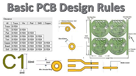
When creating PCB artwork, it is essential to adhere to a set of design rules and constraints. These rules ensure that the PCB can be manufactured reliably and meets the required specifications. Some key design rules to consider include:
Minimum Trace Width and Spacing
The minimum trace width and spacing depend on the manufacturing capabilities of the PCB fabricator and the desired electrical characteristics of the board. Typically, smaller trace widths allow for higher routing density but may increase manufacturing costs. The spacing between traces should be sufficient to prevent signal crosstalk and short circuits.
| Copper Weight (oz) | Minimum Trace Width (mm) | Minimum Spacing (mm) |
|---|---|---|
| 0.5 | 0.10 | 0.10 |
| 1.0 | 0.15 | 0.15 |
| 2.0 | 0.20 | 0.20 |
Hole Sizes and Pad Dimensions
The hole sizes for through-hole components and vias should be chosen based on the component lead diameter and the desired level of reliability. Pad dimensions should provide sufficient annular ring for proper soldering and mechanical stability.
| Hole Diameter (mm) | Pad Diameter (mm) | Annular Ring (mm) |
|---|---|---|
| 0.8 | 1.6 | 0.4 |
| 1.0 | 1.8 | 0.4 |
| 1.2 | 2.0 | 0.4 |
Clearance and Creepage
Clearance refers to the minimum distance between conductive features on the same layer, while creepage refers to the minimum distance between conductive features on different layers. Adequate clearance and creepage distances are necessary to prevent electrical breakdown and ensure the desired level of insulation.
| Voltage (V) | Clearance (mm) | Creepage (mm) |
|---|---|---|
| <50 | 0.1 | 0.2 |
| 50-100 | 0.2 | 0.4 |
| 100-150 | 0.3 | 0.6 |

Component Placement
Proper component placement is crucial for achieving a compact and efficient PCB layout. Here are some guidelines to follow:
Functional Grouping
Group components that are functionally related or belong to the same sub-circuit together. This helps minimize the length of interconnections and improves signal integrity.
Orientation and Alignment
Orient components in a consistent direction to facilitate assembly and visual inspection. Align components along a grid to maintain a neat and organized layout.
Thermal Considerations
Place heat-generating components, such as power regulators or high-speed processors, away from temperature-sensitive components. Provide adequate spacing and thermal relief to dissipate heat effectively.

Trace Routing
Trace routing is the process of connecting components on the PCB using conductive traces. Consider the following guidelines when routing traces:
Signal Integrity
Route critical signal traces, such as high-speed or sensitive analog signals, away from potential sources of interference. Use appropriate trace widths and spacing to maintain signal integrity and minimize crosstalk.
Power and Ground Distribution
Provide adequate power and ground distribution throughout the board. Use wider traces or copper pours for power and ground nets to minimize voltage drops and improve current-carrying capacity.
Trace Length Matching
Match the lengths of traces in differential pairs or critical signal paths to maintain signal integrity and timing relationships.
Via Usage
Vias are used to connect traces on different layers of the PCB. Consider the following guidelines when using vias:
Via Types
Use through-hole vias for simple designs or when component leads need to be soldered on both sides of the board. Use blind or buried vias for higher-density designs or to minimize the board size.
Via Placement
Place vias strategically to minimize the length of traces and improve signal routing. Avoid placing vias under components or in areas that may interfere with component placement or soldering.
Via Stitching
Use via stitching techniques to improve power and ground distribution, minimize EMI, and provide shielding for sensitive signals.
Silkscreen and Documentation
Silkscreen is the text and graphical information printed on the PCB surface. It provides important information for assembly, testing, and maintenance. Consider the following guidelines for silkscreen and documentation:
Component Designators
Include clear and legible component designators on the silkscreen to facilitate assembly and troubleshooting.
Polarity and Orientation Markers
Use polarity and orientation markers for components such as diodes, electrolytic capacitors, and connectors to ensure correct assembly.
Fiducial Markers
Include fiducial markers on the PCB to provide reference points for automated assembly equipment.
Assembly and Fabrication Notes
Include relevant assembly and fabrication notes on the silkscreen or in the documentation to provide guidance for the manufacturing process.
Design for Manufacturing (DFM)
Design for Manufacturing (DFM) is the practice of designing PCBs with manufacturability in mind. Here are some DFM considerations:
Panelization
Design the PCB to be compatible with the fabricator’s panelization requirements. Consider the panel size, tooling holes, and breakaway tabs for efficient manufacturing.
Soldermask and Silkscreen
Choose appropriate soldermask and silkscreen colors and finishes based on the manufacturing capabilities and customer requirements.
Testability
Design the PCB with testability in mind. Include test points, test pads, or boundary scan features to facilitate automated testing and debugging.
Frequently Asked Questions (FAQ)
1. What is the minimum trace width and spacing for a typical PCB?
The minimum trace width and spacing depend on the manufacturing capabilities and the desired electrical characteristics. Typically, a minimum trace width of 0.15mm and a minimum spacing of 0.15mm are achievable for a standard 1oz copper PCB.
2. How do I choose the appropriate hole sizes for through-hole components?
The hole sizes for through-hole components should be chosen based on the component lead diameter and the desired level of reliability. A general guideline is to have a hole diameter that is 0.2mm to 0.3mm larger than the lead diameter to allow for sufficient clearance and solderability.
3. What is the difference between clearance and creepage?
Clearance refers to the minimum distance between conductive features on the same layer, while creepage refers to the minimum distance between conductive features on different layers. Clearance is important for preventing electrical shorts, while creepage is important for maintaining the desired level of insulation between different voltage levels.
4. How can I ensure good power and ground distribution on my PCB?
To ensure good power and ground distribution, use wider traces or copper pours for power and ground nets. Provide adequate decoupling capacitors near power-consuming components to minimize voltage fluctuations. Use via stitching techniques to create low-impedance paths for power and ground.
5. What are some common DFM considerations for PCB artwork design?
Common DFM considerations include designing the PCB to be compatible with the fabricator’s panelization requirements, choosing appropriate soldermask and silkscreen colors and finishes, and designing the PCB with testability in mind. It is important to collaborate with the PCB fabricator early in the design process to ensure that the artwork meets their manufacturing capabilities and guidelines.
Conclusion
PCB artwork design is a critical aspect of PCB manufacturing that directly impacts the manufacturability, functionality, reliability, and cost-effectiveness of the final product. By following best practices and guidelines for design rules, component placement, trace routing, via usage, silkscreen documentation, and DFM considerations, PCB manufacturers can create high-quality PCB artwork that meets industry standards and customer requirements.
Effective communication and collaboration between the PCB designer, fabricator, and assembly team are essential for successful PCB artwork design. By understanding the manufacturing capabilities, constraints, and requirements, designers can optimize the artwork for efficient and reliable production.
As technology advances and PCB designs become more complex, it is crucial for PCB manufacturers to stay up-to-date with the latest design tools, techniques, and industry standards. Continuous learning, innovation, and adaptation are key to staying competitive in the ever-evolving world of PCB manufacturing.
By mastering the art of PCB artwork design, PCB manufacturers can deliver high-quality products that meet the demanding requirements of modern electronics applications. From consumer devices to industrial equipment and beyond, well-designed PCB artwork forms the foundation for reliable and performant electronic systems.


Leave a Reply