Introduction
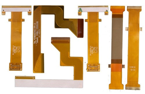
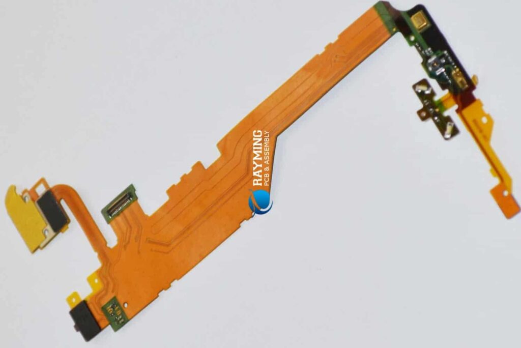
Printed circuit boards (PCBs) are essential components in electronic devices and systems. In recent years, flexible PCBs (flex PCBs) have become increasingly popular due to their durability, flexibility, and space-saving abilities. Oshpark is a well-known PCB manufacturer that offers high-quality flex PCB prototyping and small-volume production services.
In this comprehensive guide, we will cover key considerations when designing flex PCBs for Oshpark fabrication. Topics include:
- Flex PCB basics and Oshpark design rules
- Layer stackup configurations
- Trace width/spacing and bend radius
- Stiffener integration
- Testing and quality assurance
- Cost optimization
- Comparison to rigid PCBs
Whether you are new to flex PCBs or simply want a refresher on best practices, this guide aims to provide helpful tips and insight into designing successful flex PCBs with Oshpark. Let’s get started!
Flex PCB and Oshpark Basics
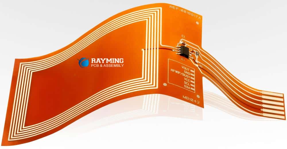
A flex PCB uses a flexible dielectric base material such as polyimide or polyester instead of the rigid FR-4 material used in traditional PCBs. The flexible nature allows the PCB to bend and flex repeatedly without damage.
Key benefits of flex PCBs:
- Can conform to fit mechanically challenging spaces
- Vibration/shock resistant
- Lightweight and portable
- Can be dynamically flexed and folded
- Low-profile and thin
Oshpark offers 2-layer and 4-layer flex PCBs with the following design rules and capabilities:
- Minimum trace/space: 6 mil
- Minimum hole size: 8 mil
- Minimum annular ring: 5 mil
- Solder mask and silkscreen options
- ENIG (gold) plating
- Panel sizes up to 13 x 19 inches
- Flex-rigid PCB combinations supported
Understanding Oshpark’s design rules and capabilities is key for creating a successful flex PCB project. Consult their online documentation for full details.
Layer Stackup Configuration
The layer stackup defines the layer structure in a PCB. For flex PCBs, common configurations are:
2 Layer
- Top silkscreen
- Top soldermask
- Copper
- Dielectric core
- Copper
- Bottom soldermask
- Bottom silkscreen
This provides a single flexible circuit layer. Minimum bend radius is defined by the dielectric material.
4 Layer
- Top silkscreen
- Top soldermask
- Copper
- Dielectric core
- Copper (inner 1)
- Core dielectric
- Copper (inner 2)
- Bottom soldermask
- Bottom silkscreen
Having two inner copper layers provides more routing capabilities. The minimum bend radius increases due to the additional copper layers.
For high-density designs, additional layers can be added. Consult Oshpark’s capabilities for the latest offerings. Carefully consider layer stackup – additional layers increase cost and minimum bend radius.
Trace Width/Spacing and Bend Radius
Two key considerations for flex PCB layout are trace width/spacing and bend radius.
Trace Width/Spacing
Oshpark requires minimum 6 mil trace/space. However, it is recommended to design for 8 mil or above when possible:
- Wider traces are more durable for dynamic bending applications
- Easier assembly for hand-soldering/rework
For controlled impedance, utilize Oshpark’s impedance calculator to optimize trace widths.
Bend Radius
The bend radius dictates the minimum radius the PCB can be bent before traces/layers may crack or delaminate.
Oshpark provides the following minimum bend radius guidance:
- 2 layer: 10x dielectric thickness
- 4 layer: 14x dielectric thickness
- 6+ layer: Consult Oshpark
Ideally, do not design traces to wrap around sharp 90 degree bends. For dynamic bending applications, increase bend radius when possible. In rigid sections of the PCB, bend radius is not a concern.
Stiffener Integration
For sections of a flex PCB that should remain rigid (like connector areas), stiffeners can be integrated:
Types of stiffeners:
- Rigid flex PCB sections: Integrate dedicated rigid PCB sections using rigid-flex PCB manufacturing
- Additional soldermask: Apply additional soldermask builds up layer thickness, increasing rigidity
- Adhesives: Bond flex PCB to rigid support structure using adhesive
Properly designed stiffeners prevent unwanted PCB bending while maintaining flexibility in other areas.
Testing and Quality Assurance
Ensuring quality and reliability requires testing flex PCBs under bending:
Suggested tests:
- Visual inspection under magnification
- Netlist testing for opens/shorts
- Impedance testing if controlled impedance designed
- Loss measurement for high-speed design
- Flattening PCBs and inspecting for damage
- Dynamic bend cycle testing
- Environmental testing (thermal, humidity)
Oshpark provides design-for-test coupons to support testing of trace durability and bend radius. Rigorous testing identifies issues prior to full production.
Cost Optimization
Like all PCB fabrication, costs increase with:
- More layers
- Tighter trace/space
- Smaller sizes
- Special materials
- Certifications
To reduce cost:
- Use 2 layers if allowable
- Design for 8+ mil trace/space
- Panelize when possible
- Stick to Oshpark’s standard offerings
- Compare pricing tiers (Hobbyist vs. Pro)
Discuss advanced requirements with Oshpark engineering to ensure manufacturability and cost-effectiveness.
Comparison to Rigid PCBs
Compared to rigid PCBs, considerations when selecting flex PCBs:
Flex PCB pros:
- Can fit challenging 3D spaces
- Vibration/shock resistance
- Dynamic flexing ability
- Lightweight and portable
Flex PCB cons:
- Generally more expensive
- Limited to 2-4 layers maximum
- Large rigid sections still need to be supported
- Lower maximum frequencies compared to rigid boards
Evaluate both flex and rigid PCB technologies when selecting the optimal solution for your design.
Frequently Asked Questions
Here are some common questions about designing flex PCBs with Oshpark:
Q: What dielectrics and thicknesses are available?
A: Oshpark offers 1.4 mil and 2.0 mil polyimide flex materials, as well as 1.6 mil adhesiveless polyimide. Contact them to discuss additional offerings.
Q: Can components be mounted on the flex PCB?
A: Yes, but ensure components do not interfere with bending zones. Use caution when mounting heavy components.
Q: What file formats does Oshpark accept?
A: Oshpark accepts Gerber, Eagle, and KiCad board formats. They also offer design rule checking.
Q: How long does manufacturing take?
A: Standard lead time is ~21 days. Expedited options are available for faster delivery.
Q: Can I order assemblies or stencils from Oshpark?
A: No, Oshpark focuses exclusively on PCB fabrication. You will need to source assembly separately.
Conclusion
Designing flex PCBs requires special considerations for layout, materials, testing, and manufacturing. By following Oshpark’s design rules and the guidelines in this article, you can create successful flex PCB prototypes and small production runs. The unique benefits of flex PCB technology make it a useful option when standard rigid PCBs are not suitable. With careful planning and rigorous verification, flex PCBs can enable innovative electronic designs in challenging form factors.


Leave a Reply