Introduction to Multilayer PCB
A multilayer printed circuit board (PCB) is a complex and advanced type of PCB that consists of multiple layers of conductive copper foil laminated together with insulating material. Unlike single or double-layer PCBs, multilayer PCBs offer higher component density, better signal integrity, and improved electromagnetic compatibility (EMC). These features make multilayer PCBs essential for modern electronic devices, including smartphones, computers, and medical equipment.
Advantages of Multilayer PCBs
- Increased circuit density
- Improved signal integrity
- Better EMC performance
- Reduced form factor
- Enhanced reliability
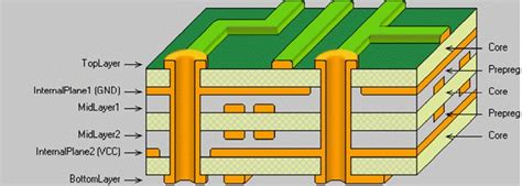
Multilayer PCB Structure
A typical multilayer PCB consists of the following layers:
- Copper layers: These are the conductive layers that form the electrical connections between components. The number of copper layers can range from 4 to 50 or more, depending on the complexity of the design.
- Insulating layers: These layers, made of materials such as FR-4 or polyimide, provide electrical isolation between the copper layers.
- Solder mask: A protective coating applied to the outer layers of the PCB to prevent short circuits and improve the durability of the board.
- Silkscreen: A layer of text and symbols printed on the PCB for component identification and assembly instructions.
Common Layer Stackups
| Layer Count | Stackup |
|---|---|
| 4 | Signal – Ground – Power – Signal |
| 6 | Signal – Ground – Signal – Signal – Power – Signal |
| 8 | Signal – Ground – Signal – Power – Signal – Ground – Signal – Signal |
| 10 | Signal – Ground – Signal – Power – Signal – Signal – Power – Signal – Ground – Signal |

Designing Multilayer PCBs
Designing a multilayer PCB involves several key considerations to ensure optimal performance and manufacturability.
Signal Integrity
Signal integrity refers to the quality of the electrical signals transmitted through the PCB. To maintain signal integrity in multilayer PCBs, designers should:
- Use controlled impedance traces
- Minimize crosstalk between adjacent layers
- Implement proper grounding and shielding techniques
- Optimize trace routing and spacing
Power Distribution Network (PDN)
A well-designed PDN is crucial for maintaining stable voltage levels and minimizing noise in multilayer PCBs. Some best practices for PDN design include:
- Using dedicated power and ground planes
- Implementing decoupling capacitors close to ICs
- Minimizing the inductance of power and ground connections
- Using via stitching to reduce impedance
Thermal Management
As multilayer PCBs pack more components into a smaller space, thermal management becomes increasingly important. Designers can improve thermal performance by:
- Using thermal vias to dissipate heat from hot components
- Selecting materials with high thermal conductivity
- Optimizing component placement for better heat distribution
- Implementing active cooling solutions, such as fans or heat sinks

Manufacturing Multilayer PCBs
The manufacturing process for multilayer PCBs is more complex than that of single or double-layer boards, involving several key steps:
- Inner layer fabrication: The individual copper layers are etched and drilled according to the design.
- Lamination: The inner layers are aligned, stacked, and bonded together under high pressure and temperature.
- Drilling: Through-holes and vias are drilled through the laminated board.
- Plating: The drilled holes are plated with copper to establish electrical connections between layers.
- Outer layer fabrication: The outer layers are etched and the solder mask and silkscreen are applied.
- Surface finish: A protective surface finish, such as HASL or ENIG, is applied to the exposed copper areas.
Key Manufacturing Considerations
To ensure a successful multilayer PCB manufacturing process, designers should keep the following considerations in mind:
- Layer registration: Proper alignment of the inner layers is critical for achieving reliable electrical connections.
- Drilling accuracy: The drilled holes must be precisely located to ensure proper connectivity between layers.
- Material selection: The choice of laminate material and copper thickness can affect the performance and manufacturability of the PCB.
- Design for manufacturing (DFM): Adhering to DFM guidelines, such as minimum trace width and spacing, can help avoid manufacturing issues and improve yield.

Testing and Quality Control
Multilayer PCBs undergo rigorous testing and quality control procedures to ensure they meet the required specifications and performance criteria.
Common Testing Methods
- Automated optical inspection (AOI): An automated system checks for visible defects, such as missing components or solder bridges.
- X-ray inspection: Used to detect internal defects, such as voids in solder joints or misaligned layers.
- Electrical testing: Verifies the electrical performance of the PCB, including continuity, insulation resistance, and high-potential (hipot) testing.
- Functional testing: Ensures the PCB performs as intended in the final application.
Quality Control Standards
Multilayer PCBs are manufactured and tested according to various industry standards, such as:
- IPC-A-600: Acceptability of Printed Boards
- IPC-6012: Qualification and Performance Specification for Rigid Printed Boards
- IPC-6013: Qualification and Performance Specification for Flexible/Rigid-Flexible Printed Boards
- IPC-A-610: Acceptability of Electronic Assemblies
Adhering to these standards helps ensure the quality and reliability of multilayer PCBs.
Applications of Multilayer PCBs
Multilayer PCBs find applications in a wide range of industries and products, including:
- Consumer electronics: Smartphones, tablets, laptops, and wearables
- Automotive: Infotainment systems, advanced driver assistance systems (ADAS), and electric vehicle (EV) power electronics
- Medical devices: Implantable devices, diagnostic equipment, and patient monitoring systems
- Aerospace and defense: Avionics, satellite communication systems, and military-grade electronics
- Industrial automation: Programmable logic controllers (PLCs), human-machine interfaces (HMIs), and robotics
As technology advances and devices become more complex, the demand for multilayer PCBs continues to grow across these industries.
Future Trends in Multilayer PCB Technology
The multilayer PCB industry is constantly evolving to meet the ever-increasing demands for higher performance, smaller form factors, and greater reliability. Some of the key trends shaping the future of multilayer PCBs include:
- High-density interconnect (HDI): HDI technology enables finer trace widths, smaller vias, and higher component density, allowing for even more compact and complex designs.
- Embedded components: Integrating passive components, such as resistors and capacitors, within the PCB layers can further reduce the form factor and improve performance.
- Advanced materials: The development of new laminate materials with improved thermal, mechanical, and electrical properties will enable multilayer PCBs to operate in more demanding environments.
- 3D printing: Additive manufacturing techniques, such as 3D printing, may revolutionize the way multilayer PCBs are designed and manufactured, offering greater design freedom and faster prototyping.
- Artificial intelligence (AI) in design: AI-driven design tools can help optimize multilayer PCB layouts, predict potential issues, and streamline the design process.
As these trends continue to shape the industry, multilayer PCBs will remain a critical component in the development of advanced electronic devices.
Frequently Asked Questions (FAQ)
1. What is the difference between a multilayer PCB and a single or double-layer PCB?
A multilayer PCB consists of three or more conductive layers, while single and double-layer PCBs have one and two conductive layers, respectively. Multilayer PCBs offer higher component density, better signal integrity, and improved EMC performance compared to single or double-layer PCBs.
2. How many layers can a multilayer PCB have?
Multilayer PCBs can have anywhere from 4 to 50 or more layers, depending on the complexity of the design and the application requirements. The most common layer counts are 4, 6, 8, and 10.
3. What materials are used in the construction of multilayer PCBs?
The most common materials used in multilayer PCBs are:
- Copper foil for the conductive layers
- FR-4 or polyimide for the insulating layers
- Solder mask for the protective coating
- Silkscreen for the text and symbols
4. What are the key considerations when designing a multilayer PCB?
When designing a multilayer PCB, engineers must consider several factors, including signal integrity, power distribution network (PDN) design, thermal management, and design for manufacturing (DFM). Proper attention to these factors ensures optimal performance and manufacturability of the PCB.
5. What are the advantages of using embedded components in multilayer PCBs?
Embedding passive components, such as resistors and capacitors, within the PCB layers offers several advantages:
- Further reduction in form factor
- Improved electrical performance
- Reduced parasitic effects
- Simplified assembly process
However, embedded components also increase the complexity and cost of the PCB manufacturing process.
Conclusion
Multilayer PCBs are essential building blocks for modern electronic devices, offering higher component density, better signal integrity, and improved EMC performance compared to single or double-layer PCBs. Designing and manufacturing multilayer PCBs involves careful consideration of factors such as signal integrity, power distribution, thermal management, and adherence to industry standards and best practices.
As technology continues to advance, the demand for multilayer PCBs will only grow, driven by the need for smaller, faster, and more reliable electronic devices. By staying informed about the latest trends and developments in multilayer PCB technology, engineers and designers can create innovative solutions that meet the evolving needs of the electronics industry.


Leave a Reply