What is PCB Depaneling?
PCB depaneling is the process of separating individual printed Circuit Boards (PCBs) from a larger panel they are manufactured on. PCBs are typically produced in arrays or panels containing multiple identical boards to improve manufacturing efficiency and reduce costs. After the PCBs are fully assembled, they need to be singulated or “depaneled” into individual boards for final assembly into electronic devices.
There are several methods used for PCB depaneling, including:
| Method | Description |
|---|---|
| V-scoring | Grooves are cut in a V-shape on the panel between boards |
| Tab routing | Tabs are left connecting boards and then cut or broken apart |
| Pizza cutting | A round blade slices boards apart like a pizza cutter |
| Laser cutting | A laser cuts out and separates individual boards |
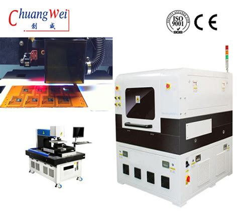
Each depaneling method has advantages and limitations based on factors like PCB material, thickness, components near the board edges, and production volume. In this article, we will focus specifically on laser cutting, which has become an increasingly popular PCB depaneling method, especially for challenging applications like rigid or Ceramic PCBs.
Advantages of Laser PCB Depaneling
Laser cutting uses a focused and high-powered laser beam to precisely cut out PCB boards from panels. It is a non-contact process, meaning the laser does not physically touch the PCB. This offers several advantages compared to mechanical cutting methods:
-
No stress on boards – Mechanical depaneling methods put physical stress on PCBs which can cause damage. Laser cutting avoids contact, vibration and stress on boards.
-
Cuts any board shape – Lasers can flexibly cut out any flat 2D board shape including with curved outlines. Mechanical methods are more limited in cutting complex shapes.
-
Smaller features and traces – The focused laser beam can cut narrower outlines, allowing smaller keep-out areas around board edges. This enables designs with finer pitch components and traces closer to board edges.
-
Less dust and debris – Mechanical routers and blades generate dust and debris as they cut. Laser cutting is cleaner with less risk of contamination.
-
Faster and automated – Laser Depaneling is a high-speed process that can be automated with handling systems, vision alignment, and job programming. This allows high volume production.
The main downsides of laser depaneling are higher equipment costs and some limitations with thicker PCBs over 2-3 mm or backplanes over 1mm thick. Lasers can also have trouble with boards containing large copper planes, as the copper reflects much of the laser energy.

Laser Depaneling Ceramic PCBs
Ceramic printed circuit boards are specialized high-performance PCBs made with a ceramic substrate material like alumina or aluminum nitride instead of the traditional FR-4 fiberglass. Ceramic PCBs offer superior thermal, mechanical and dielectric properties for applications like high-power LEDs, automotive electronics, aerospace and military systems.
However, ceramic PCBs also present challenges for depaneling due to their rigid and brittle nature. Ceramic is harder and more prone to cracking and damage under mechanical stress compared to FR-4. Ceramic PCBs also often have thicker copper, up to 400 µm or more, since they are used to conduct more power. This makes ceramic PCBs more difficult to cut mechanically without damage.
Laser cutting is an ideal depaneling method for ceramic PCBs because:
- It is non-contact and puts no stress on the brittle ceramic material
- It can handle thicker ceramic substrates and copper layers
- It can flexibly cut any flat shape including round boards
- It is fast and can be automated for volume production

Choosing a Laser for Ceramic PCB Depaneling
Several types of lasers can be used for PCB depaneling, but CO2 lasers and UV lasers are the most common in the industry.
CO2 lasers use an electrically stimulated gas mixture to generate an infrared laser beam with a wavelength around 10.6 µm. CO2 is the most popular industrial laser type with good power and efficiency. However, the long wavelength limits how small the beam can be focused for finer cutting.
UV lasers, like Nd:YAG (neodymium-doped yttrium aluminum garnet) lasers, produce a laser beam in the ultraviolet spectrum, typically 355 nm wavelength. This shorter UV wavelength can be focused to a smaller beam size under 20 µm. This allows cutting narrower outlines and processing finer features.
For ceramic PCBs, UV lasers offer the precision to make clean cuts through the rigid substrate with minimal heat affected zone (HAZ). UV wavelengths are also well-absorbed by ceramic and copper, allowing efficient cutting.
Some key specifications to look for in a UV laser for ceramic PCB depaneling include:
| Spec | Value |
|---|---|
| Wavelength | 355 nm |
| Average power | 5-20 watts |
| Pulse frequency | 20-100 kHz |
| Focused beam size | Under 20 µm |
| Galvo scan head | 50-100 mm aperture |
| Motion stage | 500 x 500 mm or larger |
| Vision system | Fiducial recognition |

Setting Up a Laser for Depaneling Round PCBs
When setting up a laser to depanel round ceramic PCBs, there are a few key considerations:
-
Fixturing – The PCB panels need to be held flat and secure during laser cutting. Vacuum fixtures are commonly used to hold down substrates. The round shape may require a custom fixture plate with a recessed pocket matching the circular outline. Avoid any fixture components that will obstruct the laser beam.
-
Programming – The laser job needs to be programmed with the correct cutting path for the round shape. This is typically done in CAD/CAM software that can import the PCB Design files. The laser power, speed, pulse frequency and number of passes needs to be set based on the ceramic material and thickness. Multiple passes are typically used to minimize heat impact.
-
Alignment – Accurate alignment is critical to cutting the boards in the right locations. Fiducial marks on the panel should be used for registration. A vision system on the laser can automatically recognize fiducials and adjust the cutting path for any offsets or distortion. This ensures consistent cutting even with variations in the panel placement.
-
Process optimization – It is important to optimize the laser settings through testing to achieve the best quality cuts. Factors to balance include cutting speed, kerf width, heat affected zone, and minimizing slag or discoloration. The laser parameters may need to be adjusted for different ceramic materials or thicknesses.
Troubleshooting Laser Depaneling Issues
Some common issues that can occur when laser cutting ceramic PCBs include:
| Issue | Cause | Solution |
|---|---|---|
| Rough cut edges | Laser power too high | Reduce power, increase speed |
| Discoloration | Heat affected zone | Reduce power, increase frequency, use more passes |
| Incomplete cuts | Insufficient power or passes | Increase power or number of passes |
| Cracks or chips | Heat stress or poor fixturing | Optimize laser settings, improve fixture |
If you encounter problems with laser depaneling ceramic PCBs, here are some troubleshooting tips:
-
Adjust laser settings – The laser power, speed, frequency and focal distance all affect the cutting quality. Try making small adjustments and test the results. Aim for the fastest speed and lowest power that still makes clean cuts.
-
Check fixture and alignment – Make sure the PCB panel is held securely and flat. Check that the laser vision system is correctly finding fiducials and compensating for any offset. Misalignment can cause inaccurate cuts or damage.
-
Inspect and maintain optics – The laser lens and mirrors should be regularly inspected and cleaned. Dirt or debris on the optics can affect laser power and cause inconsistent cutting. Follow the manufacturer’s instructions for cleaning and maintenance.
-
Monitor assist gas – Most lasers use compressed air or nitrogen as an assist gas to blow away melted material. Make sure the assist gas pressure and nozzle position are correctly set. Inconsistent gas flow can lead to dross formation or poor cut quality.
-
Test different materials – Not all ceramic PCBs are exactly the same. Different compositions or formulations may respond differently to the laser. If you change suppliers or materials, do some testing to optimize the laser parameters for best results.
Frequently Asked Questions
Can CO2 lasers be used for ceramic PCB depaneling?
CO2 lasers can be used to cut ceramic PCBs, but they may not provide the same level of precision and edge quality as UV lasers. The longer wavelength of CO2 lasers makes it harder to focus the beam to a small spot size, so the kerf width and heat affected zone may be larger. Higher power CO2 lasers may be needed for thicker ceramic or copper layers.
How much slower is laser cutting than mechanical depaneling?
In general, laser cutting is faster than mechanical methods for most PCB depaneling applications. The exact speed difference depends on many factors like material, thickness, board shape and size. Laser cutting speed is mainly limited by the power and pulse frequency. With appropriate settings, lasers can cut more than 100 mm/sec. Mechanical routing or milling is typically slower, around 30-50 mm/sec feed rate, and is limited by cutter wear and breakage.
What is the smallest gap that can be laser cut between PCBs?
The minimum gap or spacing that can be cut between PCBs on a panel depends on the focused laser beam size or kerf width. With a UV laser and precision focus optics, it is possible to achieve cut kerfs as small as 15-20 µm. However, most PCB designs use slightly larger spacing for safety. A minimum gap of 0.2 mm is typical for laser depaneling. With mechanical methods, the minimum gap is larger, often 0.5 mm or more.
How do you handle the dust and fumes from laser cutting?
Laser cutting does generate some dust, smoke and fumes as the material is vaporized. Most laser systems have integrated exhaust and filtration systems to safely extract and filter these airborne particles. Fume extraction and proper ventilation is important for operator safety and to prevent contamination. Some lasers also use assist gas like nitrogen or compressed air to help blow away debris. Proper maintenance of exhaust and filter systems is necessary.
Can laser depaneling be used for Rigid-Flex PCBs?
Yes, laser cutting works well for depaneling rigid-flex PCBs that have both rigid and flexible substrate sections. The laser can accurately cut and remove the rigid sections while avoiding damage to the flexible circuits. There are a few special considerations with rigid-flex PCBs:
- Use fixturing that supports the rigid sections while allowing flex areas to bend
- Program the laser path to only cut the rigid areas and avoid flex circuits
- Optimize laser settings for each rigid and flex material stack-up
- Check for any heat affect on the flex substrates or adhesives
With proper setup, laser depaneling can provide high quality rigid-flex PCB singulation with minimal stress or damage to the circuits.


Leave a Reply