Introduction
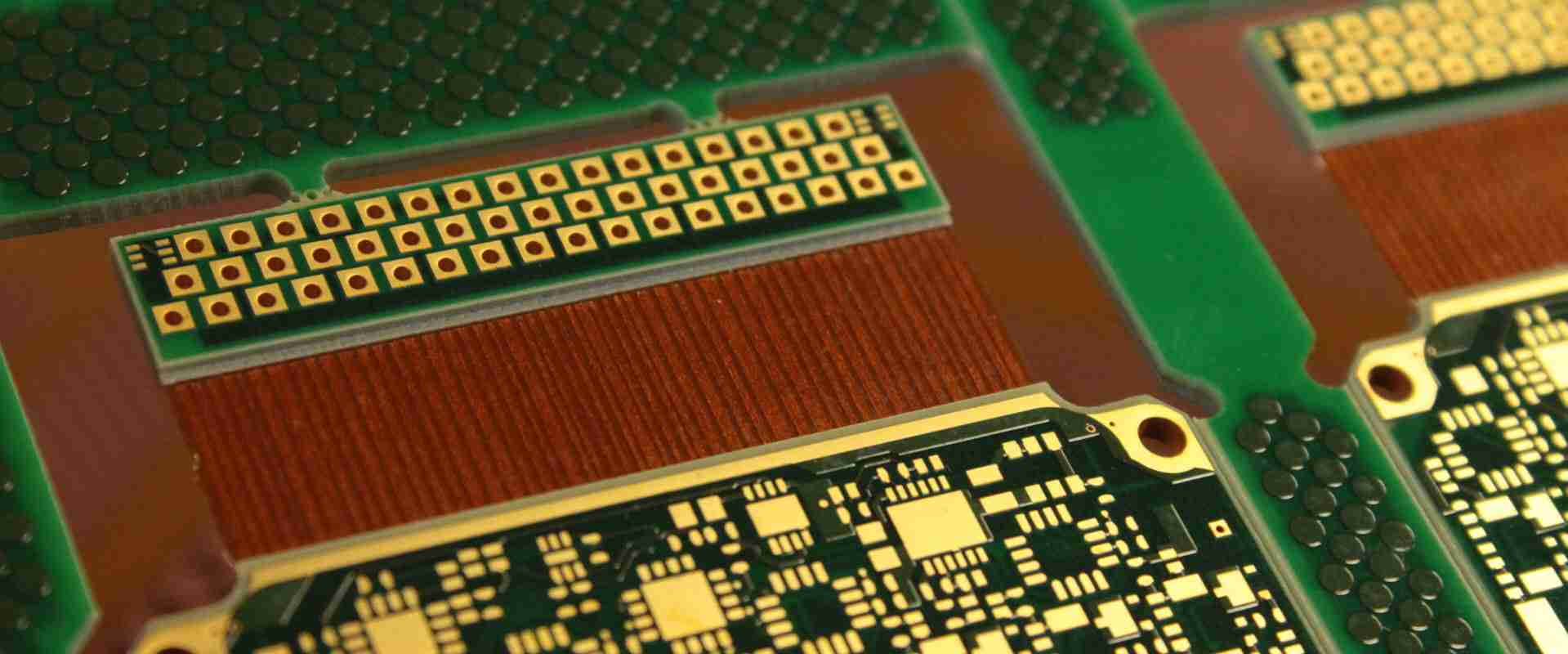
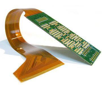
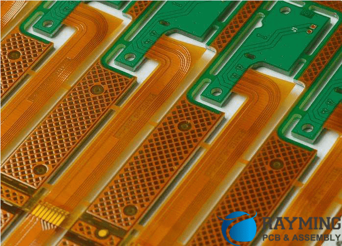
Rigid-flex PCBs combine rigid and flexible substrates to create lightweight, three dimensional circuit boards that can be customized for a wide range of applications. With KiCad, open source PCB design software, designers can create professional rigid-flex designs with advanced features like flex bends, stiffeners, and split planes. This guide will walk through the process of designing a simple rigid-flex circuit in KiCad.
Rigid-Flex Basics
Rigid-flex PCBs consist of flexible sections connected by rigid sections, allowing the boards to bend and fold in three dimensions. Here are some key terms and concepts:
- Rigid sections – Made from typical PCB substrate material like FR-4. Provides structure and component mounting.
- Flexible sections – Made from polyimide or other flexible materials. Allows bending between rigid sections.
- Flex bends – The flexible hinges between rigid sections. The minimum bend radius depends on the flex material.
- Stiffeners – Additional layers of rigid material around flex bends to prevent over-bending.
- Split planes – Power or ground planes that are split where flex bends occur to avoid cracking.
Rigid-flex has many applications such as saving space in electronics, cabling replacement, and unique form factors.
Rigid-Flex vs. Flex PCBs
Rigid-flex PCBs differ from flex PCBs which are entirely flexible except for component islands:
- Rigid-flex – Combines rigid and flexible materials for a blend of properties. Rigid areas for strength and components, flexible areas allow compact 3D shaping.
- Flex PCBs – Made solely from thin, flexible material. Mainly used for dynamic cabling applications. Requires stiffeners on components.
Designing in KiCad
KiCad supports advanced rigid-flex features, but requires some manual configuration. Here is an overview of the rigid-flex design process in KiCad:
- Create a normal PCB project
- Define rigid and flex sections under Design Rules
- Configure layer stacks for each section
- Draw rigid-flex outlines on Edge Cuts layer
- Assign sections to board outlines
- Draw gaps in copper planes at flex bends
- Add stiffeners and other rigid-flex features
The rest of this guide will walk through a simple rigid-flex design to demonstrate the process. The design has two rigid sections connected by a flexible section in the middle.
Create the PCB Project
First, create a new project and PCB. For this simple rigid-flex design, only 2 layers are needed.
After creating the PCB, you will define the rigid and flexible sections.
Define Rigid and Flex Sections
Under Design Rules, you can add rigid and flex sections:
- Open Design Rules (Design > Rules)
- Under Rigid-Flex Keywords, add:
RIGID– for rigid sectionsFLEX– for flexible sections
This defines the keywords that will be assigned to board outlines.
Configure Layer Stacks
A key part of rigid-flex design in KiCad is configuring different layer stacks for the rigid and flex sections. This allows specifying different materials and thickness for each.
To set this up:
- Open the Layer Stack Manager (Design > Layer Stack Manager)
- Create a new Layer Stack called “Rigid Layers”
- Define 2 layers of 1.6mm FR-4 material
- Create a Layer Stack called “Flex Layers”
- Define 2 layers of 0.05mm Flex material
Now you have separate layer stacks defined.
Draw Board Outlines
The board outlines define the shape of the rigid and flex sections. This is done on the Edge Cuts layer:
- On Edge Cuts layer, draw a rectangle for the main rigid section
- Draw a smaller rectangle for the second rigid section
- Draw a line connecting them for the flex section
- Assign keywords to each (Right click > Assign Keyword):
- RIGID for the two rectangles
- FLEX for the connecting line
The keywords assigned to each outline determine the sections.
Assign Layer Stacks
With the sections defined, you can now assign the layer stacks:
- Switch to the Layer Stack Manager
- For each section outline:
- Select outline
- Assign relevant layer stack (Rigid or Flex)
Each section will now have the correct material and thickness defined.
Split Planes
To avoid cracking, power and ground planes should be split where flex bending occurs.
To split planes:
- Switch to either outer copper layer
- Draw a line across the layer at the flex bend location
- Set the line to the
Splitnet
Repeat this on any layer with planes you wish to split.
Add Stiffeners
Stiffeners provide additional rigidity around flex bends to prevent over bending. They are added by drawing rigid sections slightly wider at the bends.
To add stiffeners:
- On Edge Cuts, widen the rigid sections near the flex bend
- Assign the RIGID keyword to these new outlines
- In Layer Stack Manager, assign Rigid Layers
This adds stacked rigid material for support. Multiple stiffeners can be used.
This covers the basics of a simple rigid-flex design. More complex options are possible.
Manufacturing Considerations
Here are some things to keep in mind when designing rigid-flex PCBs:
- Work closely with your manufacturer on capabilities, especially minimum bend radii.
- Avoid components near flex bends to prevent damage from repeated bending.
- Minimize rigid overlap into flex areas to prevent cracking.
- Stagger components between sides if the flex will be dynamic.
- Simpler rectangular shapes are lower cost to manufacture than complex curves.
- Expect higher fabrication costs than standard PCBs, especially for advanced HDI designs.
Example Applications
Some examples of how rigid-flex PCBs are used:
- Folding/wrapping around other components to save space
- Interconnections between multiple PCBs
- Dynamic cabling replacement
- Unique form factors, custom shapes
- Wearables and other flexible electronics
Specific products that benefit from rigid-flex:
- Laptops -Allows complex hinge routing
- Cell phones – Folds display and logic boards
- Medical devices – Match natural contours
- Robotics – Lightweight, moveable circuits
The blend of rigid and flexible materials allows for very compact and creative products.
Summary
Some key points about rigid-flex PCBs:
- Combines rigid and flexible sections for blend of properties
- Enables 3D circuit shape and compact design
- Flexible polyimide material allows dynamic bending
- Rigid sections provide structure and component mounting
- Careful design is needed for manufacturability
- KiCad allows creating advanced rigid-flex with proper setup
- Layer stacks, plane splits, and stiffeners are essential features
Rigid-flex opens up possibilities beyond normal planar PCBs. With some planning, KiCad can be used to design rigid-flex suitable for a wide range of applications.
The example project in this guide demonstrated the overall workflow. Each rigid-flex design requires customization and planning based on the requirements and manufacturing process.
FAQ
Here are some common questions about rigid-flex PCBs:
What are the main benefits of rigid-flex PCBs?
The main benefits are size reduction by folding/wrapping rigid sections connected by flexible hinges, dynamic cabling capabilities from the flex areas, and unique 3D shapes for custom products. Rigid-flex allows more compact and creative PCB implementations.
What types of products use rigid-flex PCBs?
Common applications include consumer electronics like phones and laptops, IoT and wearable devices, aerospace and automotive, and medical products. The compact folding and custom shapes rigid-flex allows are useful across many industries.
What are the downsides to rigid-flex?
The main downsides are increased complexity and cost. Rigid-flex requires special design considerations and will typically cost more to fabricate than standard PCBs, especially in lower volumes. The process also has lower yields and needs advanced manufacturing capabilities.
How durable are the flex sections?
With proper design, the flexible sections can last for thousands or tens of thousands of bend cycles. Careful control of minimum bend radius, avoiding components near flex areas, and implementing robust strain relief are key to longevity.
Can components be mounted directly on the flex sections?
In general, it’s best to avoid placing components directly in the flexible areas. They should instead be mounted to the rigid sections. If components must be placed on the flex, stiffeners are used to create islands of rigidity. Dynamic flexing requires careful component placement to avoid damage.


Leave a Reply