What are Kapton Flex PCBs?
Kapton flex PCBs, also known as flexible printed circuit boards (FPCBs), are made from a polyimide film called Kapton. Kapton has excellent electrical insulation properties while also being thin, lightweight and flexible. These properties make Kapton ideal for building circuit boards that need to bend and flex to fit into tight spaces.
Some key features of Kapton flex PCBs:
- Thin and lightweight – Kapton films can be as thin as 25 microns allowing tight bend radiuses
- Flexible – Kapton can be bent and flexed repeatedly without damage
- Durable – Withstands a wide temperature range while retaining excellent mechanical and electrical properties
- Flame retardant – Kapton meets UL-94 V-0 flammability standards
- Chemical resistant – Resists damage from most solvents, acids and oils
Kapton flex PCBs are commonly used in the following applications:
- Wearable devices – For conforming to curved surfaces like wrists
- Medical devices – For fitting into tight spaces in the body
- Consumer electronics – For folding into small gadgets like phones
- Automotive electronics – For withstanding vibration and movement
- Industrial electronics – For conforming to equipment with moving parts
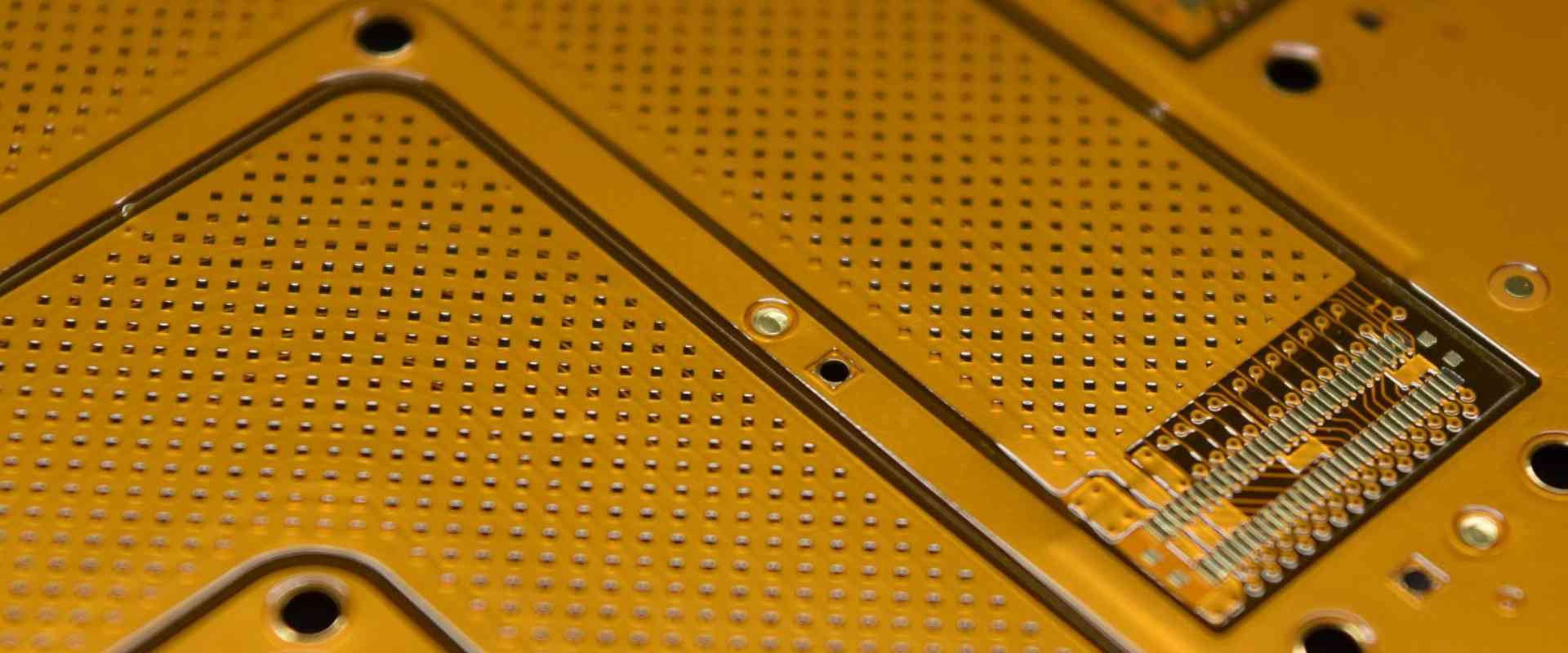
Kapton Flex PCB Construction
Kapton flex PCBs have a simpler construction than rigid PCBs, with fewer layers and components. Here are the key elements:
Kapton Base
The foundation of the PCB is a thin polyimide film. Various thicknesses are available, such as 25, 50 and 75 microns. The thinner the Kapton, the more flexible the PCB can be. However, thinner Kapton is more delicate and requires extra care in handling.
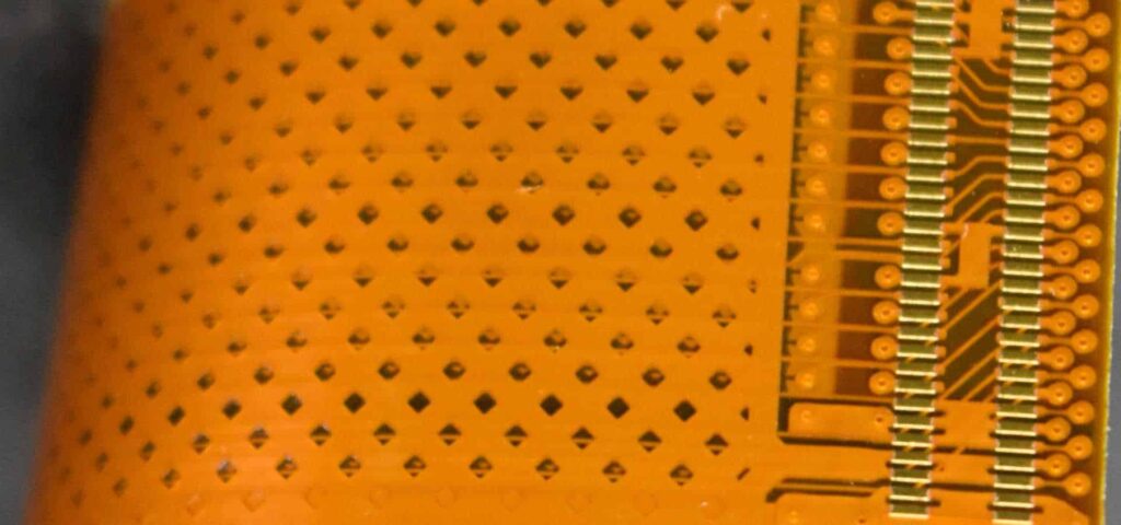
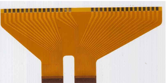
Conductive Traces
Copper traces are laminated onto the Kapton to form the conductive pathways between components. There are typically 1-2 copper layers in Kapton flex circuits. The copper is rolled annealed for maximum flexibility. The traces are also thinner than those found on rigid PCBs.
Coverlay
A coverlay is an additional layer of insulating Kapton film that goes over the copper to protect it. The coverlay has openings for electrical connections.
Bonding Adhesive
The copper traces are bonded to the Kapton base using adhesives such as acrylic, epoxy or phenolic butyral. The adhesive needs to retain adhesion during flexing. Thermosetting adhesives provide the most robust bond.
Stiffeners
Optional stiffeners made from materials like aluminum or stainless steel can be added to prevent specific areas of the PCB from bending.
Components
Components are soldered to the PCB as with any other circuit board. Typically only small surface mount devices are used to minimize thickness.
Kapton Flex PCB Design Rules
Designing a Kapton flex PCB requires following specific guidelines to ensure the circuit can flex without damage. Here are some of the critical design rules:
- Trace width – Traces must be at least 6 mils wide for better durability. 8-10 mils is recommended.
- Trace spacing – Minimum 6 mil spacing between traces.
- Bend radius – Avoid 90 degree bends. Use at least a 3mm radius bend.
- Stiffeners – Add stiffeners over components or high-stress areas.
- Adhesives – Use flexible adhesives like acrylics. Avoid rigid epoxies.
- Vias – Avoid vias in flexing sections due to potential cracking.
- Terminations – Use tear-drop terminations at solder pads for reliability.
- Components – Only use surface mount devices rated for flexing. Avoid leaded components.
Careful planning of the physical layout is critical to ensuring the flex PCB can reliably flex without components or traces cracking.
Kapton Flex PCB Manufacturing Process
Producing Kapton flex PCBs requires specialized fabrication processes tailored for flexible circuits. Here are the key manufacturing steps:
Design and Layout
The circuit is designed in CAD software. The layout focuses on trace widths, spacing, bend radii and component placement to ensure flex reliability.
Film Cutting
The Kapton polyimide film is cut into sheets of the required size. Thinner Kapton allows for tighter bend radiuses but is more fragile. 25-100 micron thickness is typical.
Copper Lamination
Rolled annealed copper foil is laminated onto the Kapton sheets using heat and adhesive. 1-2 ounce copper thickness is standard. The foil-side is coated with a UV-sensitive photoresist.
Photolithography
The circuit layout artwork is transferred to the copper using photographic techniques to expose and etch the unwanted copper. This leaves only the required conductive traces.
Etching
The unexposed photoresist is washed away, exposing the unwanted copper traces for removal by etching chemicals. This leaves only the desired circuit pattern.
Bonding
The coverlay layer is bonded over the traced Kapton core using acrylic, epoxy or other flexible adhesives. Openings are created for connections.
Testing and Finishing
The finished flex boards are electrically tested. They can then be populated with components, or supplied as bare boards. The edges are often reinforced with an epoxy encapsulation.
Kapton Flex PCB vs Rigid PCBs
Here is a comparison between Kapton flex PCBs and standard rigid PCBs:
| Parameter | Kapton Flex PCB | Rigid PCB |
|---|---|---|
| Base Material | Polyimide | FR-4 Glass Epoxy |
| Copper Thickness | 0.5 – 2 oz | 1 – 2 oz |
| Layers | 1-2 | Up to 12+ |
| Minimum Trace Width | 6 mil | 8 mil |
| Flexible | Yes | No |
| Temperature Range | -269 – 400°C | -55 – 125°C |
| Flame Retardant | Yes | Yes |
| Common Applications | Wearables, Medical, Consumer, Industrial | Computers, Communications, Consumer |
As the table illustrates, Kapton flex PCBs trade off multilayer capabilities for extreme flexibility and temperature resistance. The choice depends on the design requirements.
Kapton Flex PCB Suppliers
There are many flexible PCB manufacturers to choose from. Some of the leading global suppliers include:
- Flexible Circuit Technologies
- Minco
- All Flex
- Epec
- Eltek
- Rigid-Flex
- Flexible Circuit Solutions
- Flexible Interconnect
When selecting a flex PCB company, consider their experience, prototyping abilities, design support and budgets. Getting multiple quotes is advisable.
As flexible PCB technology has matured, costs have dropped significantly making them viable for more applications. Many PCB manufacturers can now offer budget prototyping and production of Kapton circuits.
Kapton Flex PCB Applications
Some examples of how Kapton flex PCBs are used:
Wearable Technology
Kapton flex circuits are integral to smart watches, fitness bands and health monitoring devices. The PCBs fold into the tight curves around wrists comfortably. Circuits are designed with flexing endurance in mind. Waterproofing the flexible interconnects is also critical for wearables.
Medical Devices
Medical products such as hearing aids, glucose monitors and even advanced imaging cameras utilize flex PCBs. The ability to fit Kapton circuits into tiny spaces in devices that contour to the human body make them ideal for medical uses. Biocompatibility is an important consideration for implanted devices.
Consumer Electronics
Mobile phones, displays, cameras and portable electronics depend on flexible PCBs to interconnect components in ever-smaller packages. Kapton interconnects are folded intricately to maximize space inside crowded devices. High-speed signal performance is often needed.
Automotive Applications
Kapton flex circuits are increasingly found in vehicles. Applications include LiDAR and camera-based sensors, EV battery monitoring, under-seat heating and even control panels with touchscreens. Vibration resistance, high temperatures and packaging density requirements make automotive a prime user of flexible PCBs.
With the rapid growth of wearables and IoT devices, the use of flex PCBs across industries is projected to steadily increase as new applications emerge that need compact, durable and flexible circuitry.
Kapton Flex PCB Design Software
To design a reliable Kapton flex PCB that meets the specialized flex requirements, you need an advanced PCB design tool. Here are some leading options:
Altium Designer
Flex and rigid-flex PCB design features include:
- Constraint-driven, rules-based routing for error-free flex routing
- Comprehensive flex and bend capabilities with automatic DFM checking
- Interactive flex and bend area creation and editing
- Automatic layer spanning with bridges for rigid sections
- Support for teardrops, fanouts, 4-point connections and more
- Real-time 3D clearance checking for flex clearance violations
- Integrated libraries for common flex materials, rigid sections and constraints
Cadence Allegro PCB Designer
- Constraint manager streamlines applying and controlling flex design rules
- Bi-directional bend editor supports complex bend shapes with automatic smoothing
- Interactive flex routing tools with tear drop insertion, crosshatching, and bridge connections
- Modeling of physical stackups with discrete flex materials and properties
- Automatic necking of pad shapes at rigid-to-flex transitions
- Extensive design analysis including 3D, thermal, and signal integrity
Mentor Xpedition xDX Designer
- Rules-driven rigid-flex modeling with stackup visualization
- Constraints manager enables application of bend radius rules and clearances
- Automatic rigid-to-flex shape morphing at transitions
- Interactive flex fold editing supporting simple to complex bends
- Modeling of variable bend radiuses based on stackup materials and spacing
- Built-in design rule checks (DRCs) tailored specifically to flex circuits
Board layout tools like these allow for efficient design tailored to Kapton flex PCB requirements early in the design cycle. Advanced analysis and modeling of flex materials ensures the finished boards can withstand bending stresses.
Kapton Flex PCB Considerations
Here are some important design and manufacturing considerations when working with Kapton flex PCBs:
- Component placement – Ensure components are placed only in rigid areas of the PCB. Avoid placing them in flexing zones.
- Strain relief – Provide adequate anchor points at board edges to reduce strain on traces.
- Adhesives – Use flexible adhesives like acrylics to maintain bond strength during flexing.
- Bend radius – Do not bend Kapton sharper than a 3-4mm radius. Go with larger radii when possible.
- Trace thickness – Use thicker copper (2 oz+) for longer lifetime, or annealed 1 oz. for tighter bends.
- Reinforcement – Consider edge reinforcement such as bars or encapsulation to reduce fraying.
- ESD protection – Kapton doesn’t dissipate static well, so include ground planes to avoid discharge damage.
- Shielding – Add metallic layers or enclosures if RF shielding is required. Kapton allows EMI penetration.
- Handling – Take care when handling thin flex circuits to avoid tearing or warping. Use framing and protection layers when necessary.
By following design guidelines, leveraging advanced PCB software tools, and partnering with experienced flex PCB manufacturers, you can successfully integrate Kapton flex circuits into your products. The unique benefits of flexible printed circuit boards make them ideal for many modern electronic devices and applications.
Kapton Flex PCBs FAQs
Here are some frequently asked questions about Kapton flex PCBs:
Q: How many times can a Kapton flex PCB be flexed before failing?
A: Properly designed Kapton flex PCBs can withstand 100,000+ flex cycles before traces may start to fatigue and fail. With adequate anchor points, careful bend radii and robust adhesives, Kapton flex life can meet the requirements of most applications.
Q: Can components be mounted on both sides of a Kapton flex PCB?
A: Yes, components can be surface mounted to both sides of a Kapton flex circuit. This allows for higher circuit density. Care must be taken to ensure clearance between opposing components during flexing. 3D modeling of the populated board can validate space requirements.
Q: What are some alternatives to Kapton for flexible PCBs?
A: Other common flex circuit dielectric materials include polyester (PET), polyimide (PI), polyethylene (PE) and polyphenylene sulfide (PPS). Kapton combines flexibility, heat resistance, chemical resistance and dielectric properties making it the most popular choice for demanding flexible applications.
Q: How small can Kapton flex PCB traces and spaces be?
A: Typical flex PCBs have 6 mil minimum trace widths and spaces. However, some rigid flex circuits go down to 3-4 mil traces by using 1/2 or 1/3 oz copper foils. Finer geometries require specialized imaging and etching processes.
Q: Can RF/microwave circuits be designed on Kapton flex PCBs?
A: Yes, Kapton can support gigabit speed RF and microwave signals. Controlled impedance traces with adequate dielectric spacing and shielding allow high frequency performance. Polyimide has stable electrical properties under flexing making it suitable for microwave antenna circuits.
Q: How are components attached to Kapton flex PCBs?
A: Surface mount soldering is used to attach components to Kapton flex PCBs. Reflow or hot bar soldering are common techniques. Conductive epoxy or isotropic adhesive can also be used. Care must be taken to avoid excessive heat deformation of the thin flex circuit.
Conclusion
Kapton’s unique combination of electrical insulation, thinness, light weight and flexibility make it an ideal material for constructing flex PCBs for challenging modern applications. Rigorous design principles must be followed to ensure the circuits can reliably withstand repeated flexing without failure. With the right design approach, an experienced manufacturer, and appropriate component selection, Kapton flex PCBs provide an indispensable interconnect solution for the demanding environments found in wearables, medical devices, consumer gadgets, automotive electronics and more.


Leave a Reply