Introduction to KiCad and DRC
KiCad is a popular open-source electronic design automation (EDA) software suite used for designing printed circuit boards (PCBs). It provides a set of tools for schematic capture, PCB Layout, and design rule checking (DRC). DRC is a critical step in the PCB design process that verifies the design meets manufacturability requirements and catches potential issues before sending the board out for fabrication.
One common DRC issue that designers encounter in KiCad is related to ground planes. A ground plane is a large copper fill area on a PCB layer that provides a low-impedance return path for signals and helps with electromagnetic interference (EMI) shielding. However, improperly set up ground planes can trigger DRC errors and cause problems during manufacturing.
Understanding Ground Planes in PCB Design
What is a Ground Plane?
A ground plane is a continuous copper fill area on a PCB layer, typically connected to the circuit’s ground (GND) net. Its purpose is to:
- Provide a low-impedance return path for signals
- Reduce electromagnetic interference (EMI) by shielding
- Improve power delivery by lowering the impedance between power and ground
- Help with heat dissipation
Ground planes are commonly used on multi-layer PCBs, often occupying an entire layer or a significant portion of a layer.
Benefits of Using Ground Planes
Incorporating ground planes in PCB designs offers several advantages:
-
Signal Integrity: Ground planes provide a low-impedance return path for signals, minimizing the loop area and reducing electromagnetic emissions. This helps maintain signal integrity and reduces crosstalk between adjacent traces.
-
EMI Reduction: By acting as a shield, ground planes help contain electromagnetic fields generated by the circuitry, reducing EMI emissions from the PCB. This is particularly important for designs with high-speed digital signals or sensitive analog circuits.
-
Power Delivery: Ground planes lower the impedance between power and ground, allowing for better power delivery to components. This is especially beneficial for devices with high current requirements or fast switching speeds.
-
Thermal Management: The large copper area of a ground plane helps dissipate heat generated by components on the PCB, improving thermal performance and reliability.
Designing with Ground Planes
When designing a PCB with ground planes, consider the following guidelines:
-
Placement: Allocate dedicated layers for ground planes, typically adjacent to power planes or signal layers. This proximity helps reduce the loop area and improves the return path for signals.
-
Clearance: Ensure adequate clearance between the ground plane and other copper features, such as traces, pads, and vias. The clearance requirements depend on the PCB manufacturer’s capabilities and the design’s electrical requirements.
-
Connections: Use vias to connect ground planes across different layers, providing a low-impedance path for return currents. Place ground vias near signal vias to minimize the loop area.
-
Segmentation: In some cases, it may be necessary to segment the ground plane to isolate different sections of the circuit or to control return current paths. Use caution when segmenting ground planes, as it can affect signal integrity and EMI performance.
-
Slot consideration: Be mindful of slots or cutouts in the ground plane, as they can impact signal integrity and EMI. If necessary, use stitching vias along the edges of slots to maintain continuity.
By following these guidelines and considering the specific requirements of your design, you can effectively incorporate ground planes into your PCBs and reap their benefits.

Common DRC Issues with Ground Planes in KiCad
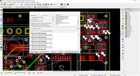
When running DRC on a PCB design with ground planes in KiCad, several issues may arise:
1. Clearance Violations
One of the most common DRC issues related to ground planes is clearance violations. This occurs when the distance between the ground plane and other copper features, such as traces, pads, or vias, is less than the specified clearance rule.
Example DRC error message:
Clearance violation between Copper Area (Pour) POWER (68.453 mm,48.006 mm) on GND and Track (68.580 mm,42.926 mm)(68.580 mm,43.307 mm) on Signal layer Top [Netclass: Default] [Severity: Medium] [Ignore DRC: No] [Track: 0.250 mm] [Vias: 0.800 mm / 0.400 mm] [Pads: 0.031 mm] [Copper/Dimension: 0.200 mm] [Drills: 0.020 mm] [Holes: 0.020 mm]
To resolve clearance violations:
- Adjust the clearance rules in the DRC settings to match the PCB manufacturer’s specifications.
- Modify the ground plane outline to provide adequate clearance around other copper features.
- Move or resize other copper features to maintain the required clearance from the ground plane.
2. Isolated Copper
Another common issue is the presence of isolated copper areas within the ground plane. These are regions of the ground plane that are not connected to the main ground net, often due to incorrect net assignments or missing connections.
Example DRC error message:
Isolated copper: Copper area (Pour) POWER on GND (68.580 mm,42.926 mm) is not connected to any net.
To resolve isolated copper issues:
- Ensure that all copper areas intended to be part of the ground plane are assigned to the correct net (usually GND).
- Check for missing via connections between ground planes on different layers.
- Verify that the ground plane outline fully encompasses the desired area and does not have unintended gaps or cutouts.
3. Starved Thermal Reliefs
Thermal reliefs are copper connections between pads and the surrounding ground plane that help dissipate heat during soldering. If the thermal reliefs are too small or missing, it can lead to starved thermal relief DRC errors.
Example DRC error message:
Starved thermal relief: Pad R1-1(68.072 mm,45.466 mm) on Top layer has insufficient thermal relief copper. [Severity: Medium] [Ignore DRC: No] [Track: 0.250 mm] [Vias: 0.800 mm / 0.400 mm] [Pads: 2.000 mm] [Copper/Dimension: 0.200 mm] [Drills: 0.900 mm] [Holes: 0.900 mm]
To resolve starved thermal relief issues:
- Adjust the thermal relief settings in the DRC rules to ensure adequate copper connection between pads and the ground plane.
- Modify the pad properties to enable thermal reliefs and set the appropriate spoke width and gap settings.
- Check that the ground plane copper is not too close to the pads, preventing proper thermal relief formation.
4. Acid Traps
Acid traps are small, isolated areas of copper within the ground plane that can trap acid during the PCB manufacturing process, leading to etching issues and potential reliability problems.
Example DRC error message:
Acid trap: Copper area (Pour) POWER on GND (68.580 mm,42.926 mm) has an acid trap. [Severity: Medium] [Ignore DRC: No] [Track: 0.250 mm] [Vias: 0.800 mm / 0.400 mm] [Pads: 0.031 mm] [Copper/Dimension: 0.200 mm] [Drills: 0.020 mm] [Holes: 0.020 mm]
To resolve acid trap issues:
- Identify and remove small, isolated copper areas within the ground plane that can trap acid during manufacturing.
- Ensure that the ground plane has a continuous, uninterrupted flow without small cutouts or gaps.
- Use the “Remove dead copper” option in the copper pour properties to automatically remove isolated copper areas.
By addressing these common DRC issues related to ground planes, designers can ensure that their PCBs are manufacturable and less likely to encounter problems during fabrication and assembly.

Resolving DRC Issues with Ground Planes in KiCad
When encountering DRC issues related to ground planes in KiCad, follow these steps to resolve them:
-
Review DRC Rules: Open the DRC rules settings and verify that the clearance, width, and other relevant rules are set correctly according to the PCB manufacturer’s specifications. Adjust the rules if necessary.
-
Inspect Ground Plane Outline: Check the ground plane outline for any unintended gaps, cutouts, or isolated areas. Ensure that the outline fully encompasses the desired area and is continuous.
-
Verify Net Assignments: Confirm that all copper areas intended to be part of the ground plane are assigned to the correct net (usually GND). Update any incorrect net assignments.
-
Check Connections: Look for missing via connections between ground planes on different layers. Add vias as needed to ensure proper connectivity.
-
Adjust Clearances: If clearance violations persist, modify the ground plane outline to provide adequate clearance around other copper features. Move or resize traces, pads, and vias to maintain the required clearance.
-
Enable Thermal Reliefs: For starved thermal relief issues, enable thermal reliefs in the pad properties and set the appropriate spoke width and gap settings. Ensure that the ground plane copper is not too close to the pads, preventing proper thermal relief formation.
-
Remove Acid Traps: Identify and remove small, isolated copper areas within the ground plane that can trap acid during manufacturing. Use the “Remove dead copper” option in the copper pour properties to automatically remove isolated copper areas.
-
Rerun DRC: After making the necessary adjustments, rerun the DRC to check if the issues have been resolved. If any errors persist, repeat the process and make further modifications as needed.
-
Consult PCB Manufacturer: If you are unsure about specific DRC rules or encounter issues that cannot be easily resolved, consult your PCB manufacturer for guidance. They can provide recommendations based on their manufacturing capabilities and experience.
By following these steps and iteratively resolving DRC issues, designers can ensure that their PCBs with ground planes are manufacturable and compliant with the required specifications.

Best Practices for Designing with Ground Planes in KiCad
To minimize the occurrence of DRC issues and ensure optimal performance when designing with ground planes in KiCad, consider the following best practices:
-
Plan Layer Stackup: Carefully plan your PCB layer stackup, allocating dedicated layers for ground planes. Place ground planes adjacent to power planes or signal layers to reduce loop area and improve Return Paths.
-
Set Appropriate Clearance Rules: Define clearance rules in the DRC settings that match the PCB manufacturer’s specifications. This includes clearances between the ground plane and other copper features like traces, pads, and vias.
-
Use Copper Pours: Utilize copper pours to create ground planes in KiCad. Assign the appropriate net (usually GND) to the copper pour and set the desired outline and connection settings.
-
Provide Adequate Clearance: When drawing the ground plane outline, ensure sufficient clearance around other copper features to avoid DRC violations. Use the “Outline clearance” option in the copper pour properties to automatically maintain a specified clearance.
-
Connect Ground Planes: Use vias to connect ground planes across different layers, providing a low-impedance path for return currents. Place ground vias near signal vias to minimize loop area.
-
Enable Thermal Reliefs: Configure pads to have thermal reliefs when connected to the ground plane. Set the appropriate spoke width and gap settings to ensure proper heat dissipation during soldering.
-
Avoid Acid Traps: Prevent acid traps by ensuring a continuous, uninterrupted ground plane flow. Remove small, isolated copper areas that can trap acid during manufacturing by using the “Remove dead copper” option in the copper pour properties.
-
Consider Segmentation: If necessary, segment the ground plane to isolate different sections of the circuit or control return current paths. However, be cautious when segmenting, as it can impact signal integrity and EMI performance.
-
Run DRC Frequently: Regularly run DRC checks during the design process to catch and resolve issues early. This iterative approach helps identify and address problems before they propagate further in the design.
-
Review and Verify: Before finalizing the design, carefully review the ground plane setup, checking for any missed connections, clearance violations, or isolated copper areas. Verify that the design meets the PCB manufacturer’s specifications and guidelines.
By following these best practices and paying attention to the specific requirements of your PCB design, you can effectively incorporate ground planes in KiCad while minimizing the risk of DRC issues and ensuring optimal performance.
FAQ
1. What is the purpose of a ground plane in PCB design?
A ground plane serves several purposes in PCB design:
– It provides a low-impedance return path for signals, reducing electromagnetic emissions and improving signal integrity.
– It acts as a shield, helping to contain electromagnetic fields generated by the circuitry and reducing EMI emissions.
– It lowers the impedance between power and ground, allowing for better power delivery to components.
– It helps dissipate heat generated by components on the PCB, improving thermal performance and reliability.
2. What are some common DRC issues related to ground planes in KiCad?
Common DRC issues related to ground planes in KiCad include:
– Clearance violations: When the distance between the ground plane and other copper features is less than the specified clearance rule.
– Isolated copper: Regions of the ground plane that are not connected to the main ground net, often due to incorrect net assignments or missing connections.
– Starved thermal reliefs: Insufficient copper connections between pads and the surrounding ground plane, affecting heat dissipation during soldering.
– Acid traps: Small, isolated copper areas within the ground plane that can trap acid during the PCB manufacturing process, leading to etching issues and potential reliability problems.
3. How can I resolve clearance violations between the ground plane and other copper features?
To resolve clearance violations between the ground plane and other copper features:
– Adjust the clearance rules in the DRC settings to match the PCB manufacturer’s specifications.
– Modify the ground plane outline to provide adequate clearance around other copper features.
– Move or resize other copper features to maintain the required clearance from the ground plane.
4. What should I do if I encounter isolated copper areas within the ground plane?
If you encounter isolated copper areas within the ground plane:
– Ensure that all copper areas intended to be part of the ground plane are assigned to the correct net (usually GND).
– Check for missing via connections between ground planes on different layers.
– Verify that the ground plane outline fully encompasses the desired area and does not have unintended gaps or cutouts.
– Use the “Remove dead copper” option in the copper pour properties to automatically remove isolated copper areas.
5. How can I ensure proper thermal relief when connecting pads to the ground plane?
To ensure proper thermal relief when connecting pads to the ground plane:
– Adjust the thermal relief settings in the DRC rules to ensure adequate copper connection between pads and the ground plane.
– Modify the pad properties to enable thermal reliefs and set the appropriate spoke width and gap settings.
– Check that the ground plane copper is not too close to the pads, preventing proper thermal relief formation.
By understanding and addressing these common questions related to ground planes and DRC issues in KiCad, designers can create PCBs that are manufacturable, reliable, and compliant with industry standards.
Conclusion
Ground planes play a crucial role in PCB design, offering benefits such as improved signal integrity, reduced EMI, better power delivery, and enhanced thermal management. However, improperly set up ground planes can trigger DRC errors and lead to manufacturability issues.
When designing with ground planes in KiCad, it is essential to be aware of common DRC issues, such as clearance violations, isolated copper areas, starved thermal reliefs, and acid traps. By understanding the causes and resolution methods for these issues, designers can effectively troubleshoot and address them during the design process.
To minimize the occurrence of DRC issues and ensure optimal performance, follow best practices when designing with ground planes in KiCad. These include careful layer stackup planning, setting appropriate clearance rules, using copper pours, providing adequate clearance, connecting ground planes across layers, enabling thermal reliefs, avoiding acid traps, considering segmentation when necessary, running DRC checks frequently, and thoroughly reviewing and verifying the design before finalizing.
By staying vigilant about potential DRC issues, applying best practices, and collaborating with PCB manufacturers when needed, designers can successfully incorporate ground planes into their KiCad PCB designs while ensuring manufacturability, reliability, and compliance with industry standards.


Leave a Reply