What is PCB Etching?
PCB etching is the process of creating custom printed circuit boards (PCBs) by selectively removing copper from a copper-clad board using a chemical etchant solution. This allows you to create the copper traces and pads that electrically connect components on the PCB.
PCB etching is commonly done as a DIY method to quickly prototype PCB designs or create small batches of custom PCBs without the cost and lead time of sending the designs out for professional fabrication. With some relatively inexpensive materials and tools, you can etch your own PCBs at home.
Materials Needed for PCB Etching
To etch your own PCBs, you will need the following materials:
| Material | Description |
|---|---|
| Copper clad board | A fiberglass board with a thin layer of copper bonded to one or both sides. Available in various sizes and copper weights. |
| Etchant solution | A chemical solution, typically ferric chloride or ammonium persulfate, that dissolves exposed copper. |
| Etchant tank | A plastic or glass container to hold the etchant solution during etching. Should be slightly larger than your PCB. |
| Cleaning pad | A Scotch-Brite pad or similar abrasive pad to clean the copper surface before applying etch resist. |
| Etch resist | A material applied to the copper to prevent etching and define the traces. Can be a special resist pen, paint, or transfer film. |
| Drill | A small drill or rotary tool to drill holes for component leads and vias. Carbide drill bits are recommended. |
| Protective gloves | Chemical resistant gloves to protect your hands when handling etchant. Nitrile or neoprene gloves work well. |
| Safety goggles | Protective eyewear to shield your eyes from chemical splashes. |
Choosing the Right Copper Clad Board
Copper clad boards come in a few different materials, thicknesses, and copper weights. The most common materials are:
- FR-4 fiberglass – A rigid, durable, flame-retardant material. Best for general purpose PCBs.
- Phenolic paper – A low-cost, less durable material. Suitable for simple, low-frequency circuits.
- Aluminum – An uncommon specialty material used when the PCB must dissipate heat. Requires special handling.
Standard thicknesses range from 0.031″ to 0.062″ (0.8mm to 1.6mm). 0.062″ is the most common thickness.
Copper weight refers to the thickness of the copper layer and is specified in ounces per square foot. 1 oz/ft² is most common for DIY etching. 2 oz/ft² provides better current carrying capacity but takes longer to etch.

Preparing the PCB Design
Before you can etch a PCB, you need to design the circuit and lay out the physical board. PCB design is a broad topic beyond the scope of this article, but here is a basic overview of the process:
- Create a schematic diagram of your circuit using a schematic capture program or pencil and paper.
- Decide on the physical size and shape of your PCB based on your enclosure and component sizes.
- Lay out the component footprints and copper traces using a PCB layout program. Make sure to follow design for manufacturing (DFM) guidelines.
- Export the PCB layout in a format that can be used to create the etch resist mask, such as a PDF or image file.
There are many free and low-cost PCB design tools available, such as KiCad, EasyEDA, Eagle, and Altium CircuitMaker. Some are even web-based so you don’t need to install any software.

Transferring the Design to the PCB
Once you have your PCB design ready, you need to transfer it to the copper clad board so that you can selectively etch away the unwanted copper. There are a few different methods to apply etch resist:
Etch Resist Pen
Probably the simplest method for simple designs is to draw directly on the copper using a special etch resist pen. These pens dispense an oil-based opaque black ink that is impervious to the etchant solution.
To use an etch resist pen:
1. Clean the copper surface with an abrasive pad and wipe with acetone or alcohol to remove any oils or contamination.
2. Print out your PCB layout on regular paper at actual size (1:1 scale).
3. Secure the printout to the copper using tape along one edge so that it forms a hinge.
4. Place the board on a flat surface, lift the paper using the tape hinge, and carefully draw over the printout with the resist pen, tracing all the pads and traces. Use a straightedge for long traces.
5. Remove the paper printout and touch up any incomplete or rough areas with the pen.
An etch resist pen works well for simple single-sided boards but requires a steady hand. The resulting traces tend to be fairly wide so this method is not suitable for designs with fine pitch traces or surface mount components.
Laser Printer Toner Transfer
For more complex designs, a popular DIY method is to use a laser printer and glossy paper to transfer toner to the copper as an etch resist mask. The toner transfer process is as follows:
- Clean the copper surface with an abrasive pad and wipe with acetone or alcohol.
- Print a mirrored (flipped horizontally) version of your PCB layout onto glossy paper using a laser printer. Use the best quality setting and consider printing multiple copies for a thicker toner deposit.
- Cut out the printed design leaving about a ¼” margin around the edges of the board outline.
- Place the copper board copper side up on an ironing board or heat-safe surface. Position the laser printout toner side down on top of the copper.
- Carefully iron the back of the printout using a hot clothes iron set to the highest cotton setting (no steam). Apply firm even pressure for 5-10 minutes until the entire printout is adhered to the copper.
- Allow the board to cool, then soak it in water for a few minutes until the paper is thoroughly wet. Carefully peel off the paper backing, leaving just the toner on the copper.
- Touch up any missing or damaged areas of the toner mask using an etch resist pen or paint.
With some practice and experimentation, laser printer toner transfer can produce reliable, high-resolution etch resist masks suitable for both through-hole and surface mount designs. The keys to success are getting the ironing temperature and pressure right and not moving the paper while ironing.
Photo Etching
For the highest resolution, most professional-looking results, you can use photosensitive etch resist and expose it using UV light, similar to how photographic film is developed. Photo etching requires additional materials and equipment compared to toner transfer or resist pens:
| Material | Description |
|---|---|
| Pre-sensitized copper boards | Copper clad boards with a light-sensitive resist coating applied. Available in positive and negative acting varieties. |
| Photo resist developer | A chemical solution, typically sodium hydroxide (lye) or potassium carbonate, that dissolves the unexposed areas of the photo resist. |
| Transparency film | A clear plastic film that can be printed with a laser printer or photocopier to create the exposure mask. |
| Exposure unit | A UV light source designed to expose the photo resist. Can be purchased or built using UV LED strips and a timer. |
The photo etching process is:
- Print your PCB layout onto a transparency film using a laser printer or photocopier. Make sure to choose the right polarity (positive or negative) based on your photo resist type.
- Place the transparency on top of the photo resist copper board in a UV exposure unit, with the printed side of the transparency against the photo resist.
- Expose the board for the recommended time according to the photo resist manufacturer’s instructions, typically 1-5 minutes.
- Develop the exposed board in the photo resist developer solution according to the manufacturer’s instructions, typically 1-2 minutes. The unexposed areas of the resist will dissolve away.
- Rinse the developed board with water and inspect the resist mask for any defects. Touch up as needed with an etch resist pen.
- Etch and drill the board as usual.
Photo etching takes more time and effort to set up than other methods, but it is the go-to process if you need to produce professional quality PCBs with fine traces and high resolution features. Pre-sensitized boards and photo resist developer have a limited shelf life, so this process is better suited for frequent PCB makers.

Etching the PCB
With your etch resist mask applied, you are ready to dissolve the unmasked copper using the etchant solution. The most common etchant solutions are:
- Ferric chloride (FeCl₃) – The traditional PCB etchant. Relatively safe and easy to use but can be messy and stain surfaces.
- Ammonium persulfate ((NH₄)₂S₂O₈) – A cleaner, less staining alternative to ferric chloride. Mixed with water, it is also known as “green etchant.”
- Cupric chloride (CuCl₂) – Another common etchant, often used in commercial PCB production. Can be regenerated by bubbling with air.
Each etchant has advantages and disadvantages in terms of etching speed, safety, disposal, and cost. Ferric chloride and ammonium persulfate are the most popular choices for DIY etching.
To etch your PCB:
1. Put on your protective gloves and goggles. Etchant solutions are corrosive and can cause chemical burns.
2. Place your resist-masked PCB into a flat bottomed plastic or glass container. An old baking dish or plastic food storage container works well.
3. Pour enough etchant solution into the container to cover the PCB by about ½”. The amount needed depends on the size of your board and container.
4. Agitate the solution by gently rocking the container or moving the PCB with tongs. This helps speed up the etching process and ensures even etching.
5. Periodically check the progress of the etching by lifting the board out of the solution. Rinse it with water to get a better look. The exposed copper should gradually dissolve away, leaving only the resist-protected traces.
6. Continue agitating and checking until all the unwanted copper is gone and only the traces remain. Etching can take anywhere from 5 to 45 minutes depending on the copper weight, etchant type, etchant temperature, and agitation.
7. When etching is complete, remove the board and rinse it thoroughly with water. Dispose of the used etchant according to your local regulations – it usually needs to be treated as hazardous waste.
8. Strip the etch resist mask off the board using acetone or a dedicated resist stripper solution. An old toothbrush can help remove stubborn spots of resist.
9. Clean and dry the board, then inspect it carefully for any defects or discontinuities in the copper traces. Make repairs with solder or conductive ink if needed.
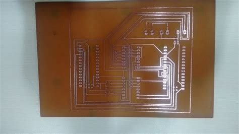
Your PCB is now ready for drilling and assembly!
Drilling and Assembling the Etched PCB
The final steps in making an etched PCB are drilling the holes for component leads and vias, and soldering the components to the board.
To drill your PCB:
1. Secure the board to a drill press table or a sacrificial backing board using double-sided tape or a light duty spray adhesive. This prevents the board from moving while drilling.
2. Load a carbide drill bit of the appropriate size into a drill press or rotary tool. A #60 drill bit (0.040″/1.0mm) is a good general purpose size for through-hole component leads.
3. Use a center punch or a nail to make a dimple at each hole location. This helps prevent the drill bit from wandering.
4. Drill each hole, using light pressure and backing the bit out frequently to clear chips. Go slowly to avoid breaking the small bits.
5. Flip the board over and lightly countersink each hole to remove any burrs around the hole edges.
6. Clean the drilled board with compressed air or a soft brush to remove any dust or debris.
With all holes drilled, you can proceed to solder your components to the board:
- Insert the component leads into the appropriate holes according to your PCB layout diagram. Bend the leads outward slightly to hold the components in place when you flip the board over.
- Flip the board component side down and solder each lead to its corresponding copper pad. Use a fine tipped soldering iron and small diameter solder, and be careful not to overheat the components or lift the pads.
- Trim the leads flush with the solder joints using wire cutters.
- Clean any flux residue off the board with isopropyl alcohol and inspect the solder joints for defects under a magnifying glass. Rework any poor joints as needed.
Congratulations, you’ve just made your own etched PCB!
FAQ
What is the best etchant for PCBs?
The best etchant depends on your needs and preferences. Ferric chloride is the most popular and readily available, but it can be messy and staining. Ammonium persulfate is a cleaner alternative that is just as effective. Cupric chloride is fast acting and can be regenerated, but is more expensive and harder to find.
How long does it take to etch a PCB?
Etching time depends on several factors, including the copper weight of the board, the strength and temperature of the etchant, and how much you agitate the solution. In general, a 1 oz/ft² board will take 15-30 minutes to etch in fresh ferric chloride or ammonium persulfate at room temperature with occasional agitation.
Can I reuse the same etchant solution multiple times?
Yes, etchant solutions can be reused until they become saturated with dissolved copper and stop etching effectively. Ferric chloride turns from golden brown to dark green as it becomes saturated, while ammonium persulfate turns from clear to blue-green. To extend the life of the etchant, you can regenerate it by adding oxygen in the form of air bubbles or hydrogen peroxide.
What is tinning and why is it done after etching?
Tinning is the process of applying a thin layer of molten solder to the copper traces after etching. This is done to prevent the copper from oxidizing and turning dull, which can make it harder to solder. Tinning also makes the PCB traces more conductive and helps protect them from corrosion. To tin a board, simply float it copper side down in molten solder or use a hot air gun and solder wire.
Can I etch double-sided PCBs at home?
Yes, you can etch double-sided PCBs using the same basic process as single-sided boards. The key difference is that you need to align the etch resist masks on both sides of the board and protect one side while etching the other. One method is to sandwich the board between two sheets of transparency film and etch one side at a time. You also need to drill any vias or through-holes and electroplate them with copper to connect the top and bottom layers.


Leave a Reply