Introduction
Printed circuit boards (PCBs) serve as the foundation of electronics products, providing the mechanical structure and electrical connections for components. While traditionally made using commercial fabrication, advances in technology now enable DIY PCB prototyping at home.
Home PCB fabrication allows rapid design iteration, customization, and cost savings. This guides covers DIY PCB techniques from creating layouts to etching boards using home equipment.
Benefits of Home PCB Prototyping
Reasons hobbyists and engineers fabricate PCBs themselves:
Faster Design Iteration
- Make changes and rev boards rapidly without relying on external fab cycle times
Customization and Experimentation
- Create fully customized boards tailored to unique needs
- Experiment with novel materials and techniques
Cost Savings
- Avoid PCB fab costs, especially for low volume prototyping
- Leverage home equipment and materials already on hand
Education
- Learn hands-on about the PCB fabrication process
- Valuable skills for electronics engineering and jobs
While home techniques have limitations, they excel for low volume, custom boards, and accelerating prototyping.
Equipment Required
Here is typical equipment needed for DIY PCB fabrication:
Computer and PCB Design Software
- PC or Mac with PCB layout software like Eagle, KiCAD, etc.
- Some software have free versions with limited features
Printer
- Laser printer capable of 1200+ dpi resolution for artwork patterns
- Inkjet may work but laser preferred for precision
Laminate and Copper Clad
- FR-4, polyimide, or other circuit board substrate materials
- Single or double sided copper clad laminate
Etching Chemicals and Supplies
- Etchant like ferric chloride, cupric chloride, etc.
- Chemical resistant trays and etching tank
- Etchant disposal/recycling capability
Photoresist Materials
- UV light source like LED or fluorescent tubes
- Liquid or dry film photoresist
- Chemicals for resist developing
Drilling/Cutting
- Small mechanical drill press or CNC for holes
- Saw like jeweler’s saw for cutting boards
Miscellaneous
- Clear acetate sheets for artwork patterns
- Chemical protection supplies – gloves, goggles, apron
- Small hand tools – craft knife, tweezers, etc.
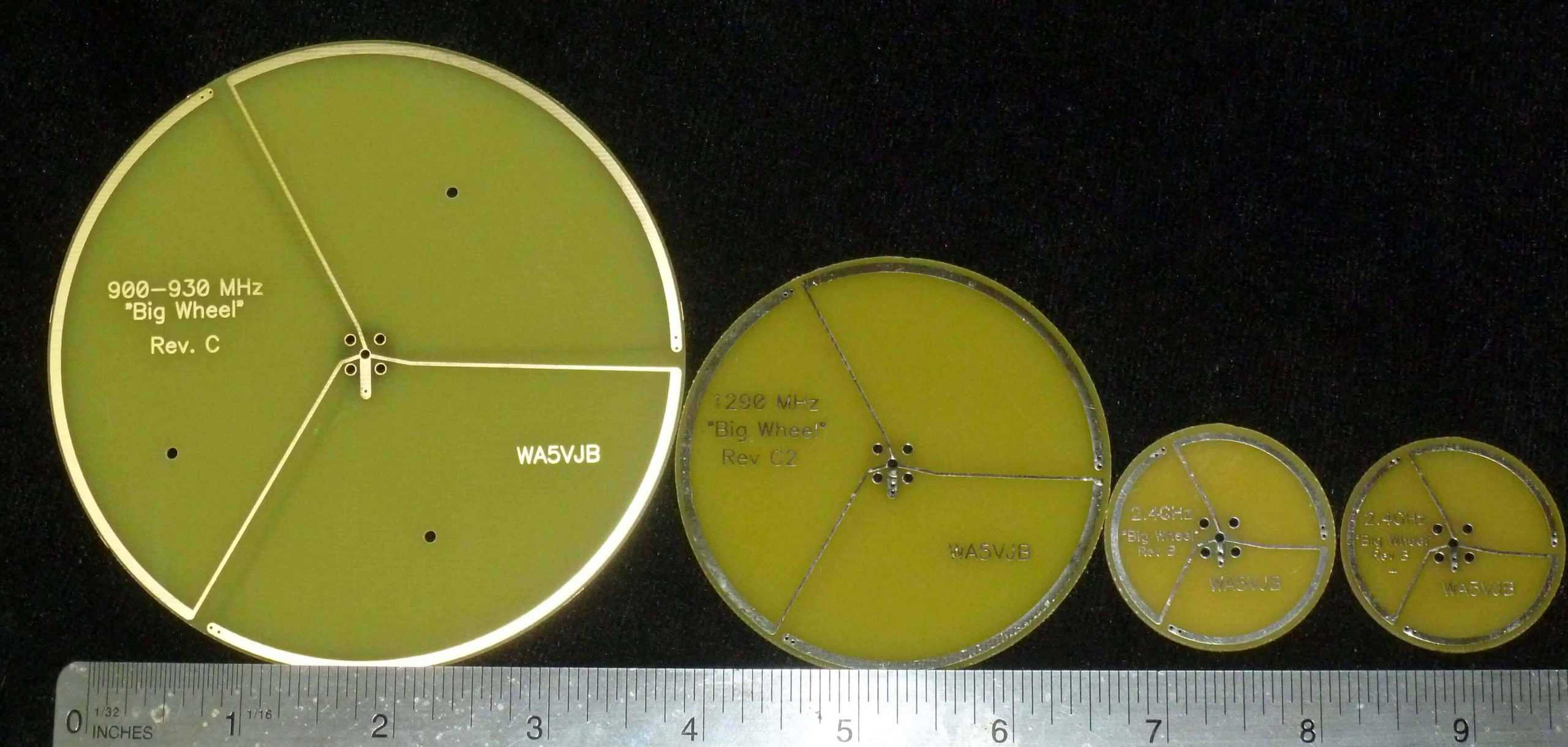
PCB Design
PCB layout tools allow customizing board designs optimized for home fabrication:
Design Rules
- Follow fabrication rules like minimum trace width and spacing
- Account for resolution limits of home etching process
Single or Double Sided
- Stick with single or double sided designs
- Avoid complex multilayer boards
Component Selection
- Select component packages usable with DIY assembly
- Avoid tiny ICs; focus on DIPs, SOICs, QFPs
Minimize Vias
- Go easy on vias requiring drilling each hole
- Rely more on jumper wires if needed
Modular Sections
- Partition complex boards into modular sections
- Easier to fabricate individually then interconnect
Panelization
- Panelize boards to max substrate size to minimize waste
- Adjust layouts and spacing for home fabrication
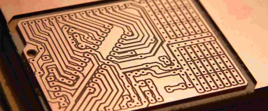
PCB Artwork Generation
The PCB layout software outputs Gerber and drill files. These are processed to generate artwork patterns:
Gerber Processing
- Use GerbMerge or similar to combine Gerber layers
- Generates composite artwork plot layer
Sizing and Spacing
- Scale and space boards in panel for available material sizes
- Add alignment targets for photo exposures
Drill Guide
- Import drill file to create drilling guide layer
- Print 1:1 scale to match PCB
Print Transparencies
- Print composite layer and drill guide onto transparencies
- Laser printer provides highest print resolution
The transparencies form artwork masks for photolithography patterning.
PCB Substrate Preparation
Preparing the PCB substrate involves cutting, cleaning, and sometimes coating:
Cutting Boards
- Cut blank laminate pieces to size using saw
- Wear respirator to control dust
Cleaning
- Clean thoroughly with isopropyl alcohol
- Removes oils and other contaminants
Surface Coating (Optional)
- May coat substrate with primer or liquid photoresist
- Improves photoresist adhesion
Proper cleaning is critical for photoresist adhesion and preventing etching defects.
Photoresist Application
Photoresist forms a mask pattern for etching away unwanted copper regions. Two options:
Liquid Photoresist
- Apply by spraying, rolling, or dipping
- Multiple coats may be needed
- Requires careful viscocity control
Dry Film Photoresist
- Layer laminated dry film onto copper surface
- Uses hot roll lamination or vacuum press
- More consistent but requires lamination tools
Whichever used, proper application ensures uniform coating without bubbles or pinholes.
Photoresist Exposure
The applied photoresist must be exposed to UV light through the mask:
Mask Alignment
- Carefully align transparencies to blank PCB
- Use alignment targets and secure in place
UV Light Source
- Fluorescent blacklight or LED exposure unit
- Place PCB directly under light panel
Exposure Time
- Typical exposure time is 2-5 minutes
- Insufficient exposure prevents full curing
A UV blocking background helps prevent reflecting light causing overexposure.
Photoresist Developing
After exposure, the resist must be developed to remove uncured regions:
Chemical Developing
- Immerse board in sodium hydroxide or potassium borates solution
- Agitate gently – developed in 1-3 minutes
- Rinse thoroughly with water
Descumming (Optional)
- Brief oxygen plasma des cumming removes residue
- Requires a plasma etching tool
This reveals the copper pattern in the cured photoresist mask.
Copper Etching
With the resist mask set, it’s time to etch away the unwanted copper:
Etchant Selection
- Ferric chloride most commonly used for home etching
- Alternatives like ammonium persulfate or nitric acid
Etching Tank
- Etchant placed in plastic or glass tank
- Use tank with lid to prevent evaporation
Temperature Control
- Elevated temperature around 50°C accelerates etching
- Use hot plate or water bath to heat tank
Agitation
- Bubble air or use pump for etchant agitation
- Ensures fresh etchant access to dissolve copper
Etch Duration
- Visually inspect periodically until copper fully cleared
- Typical etch times 10-30 minutes
Completeness of etching determines circuit conductors.
Photoresist Stripping
After etching, the remaining photoresist mask must be removed:
Chemical Stripping
- Soak board in sodium hydroxide solution
- Heat assists stripping – 60-80°C
Abrasion
- Gently wipe away residual resist using abrasive
- Use fine steel wool, brush, or sandpaper
This reveals the completed conductive pattern on the PCB.
Drilling Holes
Vias and mounting holes are drilled using a mechanical drill:
Drill Press
- Use small hobby drill press
- Drill bit sizes matched to holes
- Secure PCBs to prevent shifting
CNC Drill
- CNC router programmable for drilling
- Import drill file for automation
- Higher precision than manual drill press
Hole Walls
- Drill walls usually require cleanup
- Fine sandpaper or blade cleans up wall roughness
Careful drilling prevents enlarged holes or poor location accuracy.
PCB Finishing
Various finishing steps complete board fabrication:
Solder Mask
- Apply solder mask like liquid photoimageable or UV curable
- Areas requiring solder left exposed
Silkscreen
- Screen print legend using etching or UV cured ink
- Identifies components, logos, text
Plated Coatings
- Brush plate exposed copper with solder or tin
- Improves solderability and protects copper traces
Edge Trimming
- Carefully trim board edges to smooth using file
- Remove roughness and nicks
Thorough cleaning prepares the PCB for electronic assembly.
Pros and Cons of Home PCB Fabrication
Advantages
- Faster design iteration than reliance on external fab
- Customization for unique design needs
- Education on inner workings of fabrication
- Lower costs for prototypes and custom boards
- Leverage existing home workshop equipment
Disadvantages
- Limited to simpler board designs
- More manual process with variability
- Challenging for multilayer boards
- Lower precision and tolerances
- Requires learning fabrication techniques
- Smaller maximum board size
Understanding limitations helps set expectations when fabricating PCBs at home.
Tips for Improving Results
Suggestions for getting better outcomes DIY PCB fabrication:
- Use dedicated chemical handling equipment only for PCB work
- Closely control temperature and timing of chemical processes
- Use laser printer for artwork with highest print resolution
- Dial in exposure time specifically for UV light source intensity
- Regularly regenerate chemical baths as they degrade with use
- Agitate etching and developing solutions frequently
- Perform test exposures on scrap boards to optimize process
- Drill undersized holes for better accuracy then resin fill
- Carefully level and secure PCBs when drilling to prevent shifts
- Review fabrication guides to compare results and troubleshoot
Learning the nuances through practice leads to progressively better results.
Alternative Methods
Beyond traditional fabrication, some alternative PCB techniques:
CNC Milling
- Use CNC router to directly mill board traces
- Requires 2-4 flute carbide micro bits
- Can drill holes precisely with same tool
Inkjet Printing
- Print etch resist mask directly using inkjet
- Eliminates photolithography steps
- Resolution challenges remain
Vinyl Cutting
- Computer cut vinyl resist masks with plotter
- Lower costs but alignment is difficult
Plating on 3D Printed PCB
- 3D print a plastic board using conductive filament
- Then electroplate conductive traces
Hand Drawing
- Use etch resist pen to hand draw traces
- Tedious but enables artistic creativity
Presensitized Boards
- Purchase pre-coated boards with photoresist
- Skip coating steps but higher cost
Conclusion
Advancements in home fabrication technology now enable DIY prototyping of custom PCBs on a budget. While requiring some investment in equipment and chemicals, home PCB fabrication empowers innovation and learning.
This provides an overview of the fundamental PCB making techniques accessible at home. Leveraging these processes allows rapid design iteration, experimentation, and cost savings.
DIY PCB Fabrication FAQs
What resolution and trace widths can be achieved with home PCB fabrication?
Typical home methods allowtrace widths down to around 8 mils with care. Resolution is limited by printer dpi, photoresist curing, and etching process capabilities.
What are some good options for making PCBs at home without chemicals?
Methods like CNC milling, hand drawing with etch resist pens, vinyl cutting, and 3D printing with conductive filaments can create PCBs without requiring wet chemistry.
What safety precautions should be taken when working with PCB chemicals?
Use protective equipment like chemical goggles, nitrile gloves, and apron. Work in well ventilated area. Follow chemical safety handling procedures and dispose properly.
Should dry film or liquid photoresist be used for home PCB fabrication?
Liquid photoresist is more accessible for home use not requiring hot roll lamination. But dry film can provide more consistent resist thickness if lamination is possible.
What are some troubleshooting tips for fixing poor quality home etched PCBs?
Review entire process for deviations. Ensure proper cleaning, photoresist exposure and curing, etching completeness, drill bit condition, etc. Compare to proven processes.


Leave a Reply