Introduction
Printed circuit boards (PCBs) are thin boards made of fiberglass and copper that allow electrical components to be mechanically supported and electrically connected. PCBs come in different layer counts, from simple single sided boards to complex boards with 16 or more layers. But a common question that arises is, how thick is a 6 layer PCB?
The thickness of a PCB depends on a few key factors:
- Number of copper layers
- Copper weight (thickness)
- Dielectric/prepreg thickness between layers
- Overall board thickness tolerance
In this article, we’ll dive into the details around PCB layer stackup and explore the typical thickness dimensions of a 6 layer board.
PCB Layer Stackup

A PCB is made up of alternating layers of copper and dielectric material. The copper layers are used to create traces, pads, and planes to route signals and power. The dielectric layers provide electrical isolation between copper layers and mechanical structure.
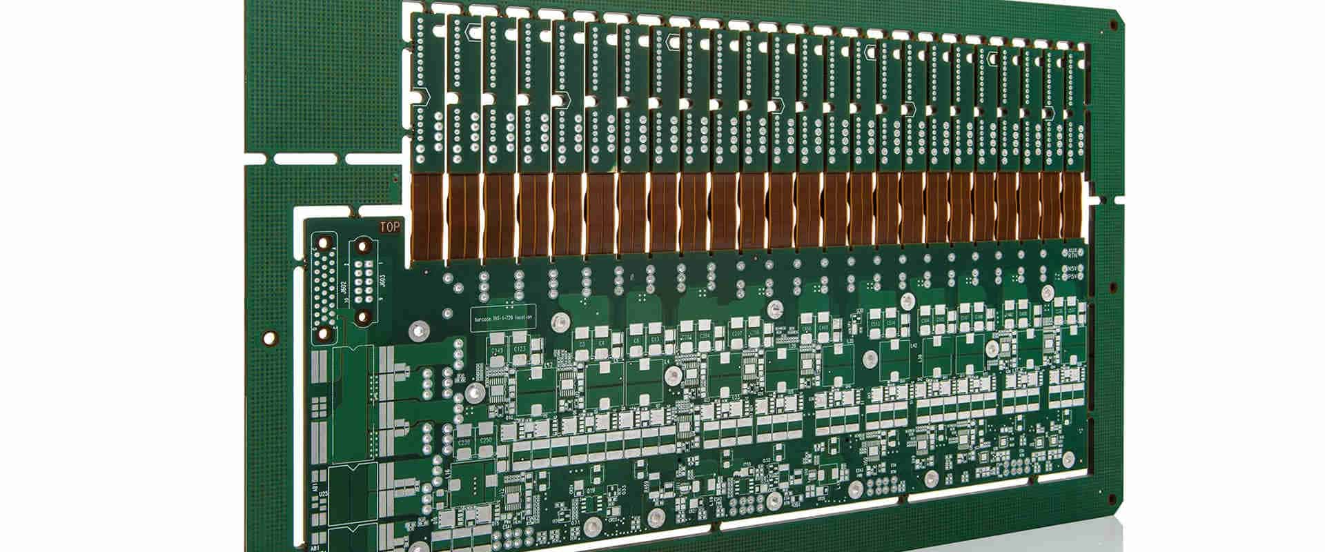
Here is a cross section depicting the layer stackup of a 6 layer PCB:
- Top and bottom outer layers (1+6) are typically signal routing layers.
- L2 and L5 are often used as power and ground planes.
- L3 and L4 can be signal layers or additional power planes.
The key dimensions we need to examine are:
- Copper thickness
- Dielectric thickness
- Overall thickness tolerance
Let’s look at each of these in more detail.
Copper Thickness
The copper layers in a PCB are usually defined by their copper weight, specified in ounces per square foot (oz/ft2). Common weights are 1 oz, 2 oz, and 3 oz. The higher the copper weight, the thicker the copper.
Here are typical thicknesses for different copper weights:
- 1 oz: 1.4 mils (0.0014 inches)
- 2 oz: 2.8 mils
- 3 oz: 4.2 mils
For a 6 layer board, 2 oz copper is typical, resulting in a thickness of 2.8 mils per copper layer.
With 6 copper layers, if we assume 2 oz thickness, the total copper thickness is:
6 layers x 2.8 mils = 16.8 mils
Dielectric Thickness
The dielectric layers provide isolation between copper layers and also determine the spacing between traces and planes. Typical dielectric materials used are FR-4, polyimide, Rogers, and others.
Dielectric thickness is usually specified in mils. Some common thicknesses are:
- 2 mil
- 3 mil
- 5 mil
For a 6 layer board, 3 or 5 mil dielectric is typical. This results in a dielectric thickness of:
5 layers x 3 mils = 15 mils (or 5 layers x 5 mils = 25 mils)
Overall Thickness Tolerance

PCB fabrication involves laminating together the stackup of alternating copper and dielectric layers. This process results in some tolerance on the overall thickness.
The thickness tolerance is usually +/- 10% of the total thickness.
So if we add together the copper and dielectric thicknesses calculated above:
- Copper: 16.8 mils
- Dielectric (3 mil): 15 mils
- Total: 31.8 mils
With a +/- 10% tolerance, the overall thickness would be:
31.8 mils +/- 3.18 mils
Or 28.62 to 34.98 mils
Summary of 6 Layer PCB Thickness
Based on the common PCB parameters examined above, here is a summary of typical 6 layer PCB thickness dimensions:
- Copper thickness: 16.8 mils (6 layers x 2.8 mils)
- Dielectric thickness: 15 or 25 mils
- Total thickness: 31.8 or 41.8 mils
- With +/- 10% tolerance: 28.6 to 34.98 mils or 37.6 to 45.98 mils
So in summary, a typical 6 layer PCB will be around 30-45 mils thick, depending on the exact materials used.
Other Factors Affecting Thickness
There are a few other factors that can influence the final thickness of a 6 layer PCB:
Board thickness requirement: Some applications may require a specified PCB thickness, which would override the typical thickness.
More dielectric/prepreg layers: Sometimes additional dielectric layers are added if more spacing is needed between copper layers. This increases the total thickness.
Thicker dielectrics: Using a thicker dielectric, like 5 or 10 mils, increases the spacing between layers.
More copper layers: Adding more copper layers adds more 2.8mils of thickness per layer.
Thicker copper: Using 3 oz or thicker copper increases the thickness per copper layer.
Board thickness tolerances: Tighter thickness tolerances (+/- 5%) result in less variance but could make fabrication more difficult.
Buried/blind vias: These specialty via types often require additional dielectric layers which adds thickness.
So in some cases, you may see 6 layer boards outside of the typical 30-45 mil range. But for standard designs, this gives a good idea of the expected 6 layer PCB thickness.
Effect of Thickness on PCB Performance
Does PCB thickness matter for performance? Here are some key considerations:
- Signal integrity: Thicker dielectric reduces capacitive coupling between traces but increases propagation delay. Must balance these effects.
- Impedance control: Thicker dielectrics allow wider trace/space and tighter impedance control. But also impacts propagation delay.
- Warpage: Thicker boards can warp more during fabrication. This can affect assembly and reliability of solder joints.
- Flexibility: Thinner boards allow more flexibility if needed. Thicker boards are more rigid.
- Thermal performance: Thicker copper helps dissipate heat, but thicker dielectric insulates more. Must balance both.
- Cost: Thicker boards require more layers and materials, increasing cost. Must justify with performance gains.
So in summary, the thickness should be designed to meet electrical, thermal, and mechanical requirements at the lowest cost. There are always tradeoffs that must be evaluated for each design.
Conclusion
To conclude, a typical 6 layer PCB with 2 oz copper and 3-5 mil dielectric will be approximately 30-45 mils thick. However, the exact thickness depends on specific design requirements and tolerance allowances. Thickness impacts signal integrity, impedance control, thermal dissipation, warpage, and flexibility. Engineers must properly balance all these factors when selecting layer stackup and materials to achieve optimal board performance at the lowest cost.
Frequently Asked Questions
What are the standard PCB thicknesses?
The most common PCB thicknesses are:
- 1.6 mm (63 mils) – Typically 2-layer or 4-layer boards
- 2.4 mm (94 mils) – Typically 6-layer or 8-layer boards
- 3.2 mm (126 mils) – Typically 8-layer and higher layer count boards
However, thickness ultimately depends on individual design requirements.
What is the typical PCB thickness tolerance?
The overall thickness tolerance is usually +/- 10% of the total board thickness. So for a 60 mil board, the tolerance would be +/- 6 mils. Tighter tolerances such as +/- 5% are possible but may increase fabrication cost.
How does thickness affect PCB cost?
Generally, thicker PCBs with more layers cost more to fabricate. Key cost drivers are:
- Number of lamination cycles
- Amount of materials (copper, dielectric)
- Tighter thickness tolerances
- Advanced processing for blind/buried vias
So thickness should be minimized as much as possible while still meeting design rules and performance requirements.
Can PCBs be too thick for assembly?
Yes, very thick boards can create issues for PCB assembly and soldering. For example:
- Tall components may not fit
- Warpage may lift boards off the assembly table
- Heat transfer through thicker boards makes soldering difficult
- Thicker boards can flex and damage solder joints
As a rule of thumb, boards over 2.5mm (100 mils) should be evaluated for assembly and soldering issues.
How does thickness affect flexibility and warpage?
Thinner boards can flex more easily. Thicker boards are more rigid but can warp more during fabrication or heating. A medium thickness around 1.6mm provides a good balance. Boards over 2.4mm tend to become too rigid and prone to warpage.


Leave a Reply