Introduction to PCB Inspection
Printed Circuit Board (PCB) inspection is a crucial step in the manufacturing process to ensure the quality and reliability of electronic devices. PCB inspection involves examining the board for various defects, such as short circuits, open circuits, incorrect component placement, and soldering issues. In this article, we will discuss the various methods and techniques used for PCB inspection.
Why is PCB Inspection Important?
PCB inspection is essential for several reasons:
-
Quality Assurance: PCB inspection helps maintain the quality of the final product by identifying and rectifying defects early in the manufacturing process.
-
Cost Savings: Detecting and fixing issues during the inspection stage is more cost-effective than dealing with product failures or recalls later.
-
Reliability: Thoroughly inspected PCBs are more reliable and have a longer lifespan, which is crucial for critical applications such as medical devices, aerospace, and automotive electronics.

Types of PCB Inspection
There are three main types of PCB inspection:
1. Visual Inspection
Visual inspection is the most basic form of PCB inspection and involves examining the board with the naked eye or using magnifying tools. This method is suitable for identifying obvious defects such as incorrect component placement, damaged components, or poor soldering.
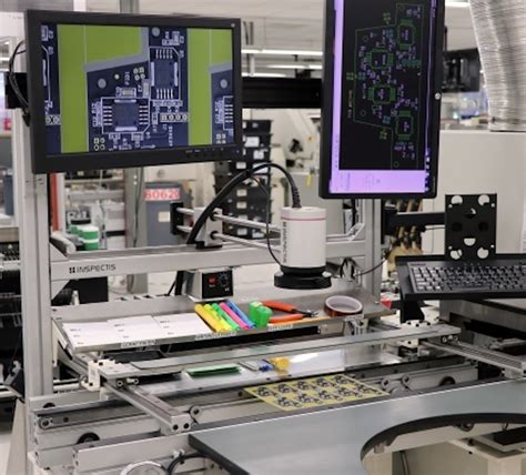
2. Automated Optical Inspection (AOI)
AOI uses high-resolution cameras and advanced image processing software to inspect PCBs. The system compares the captured images of the board with a reference image to identify any discrepancies. AOI is faster and more accurate than visual inspection and can detect subtle defects that may be missed by the human eye.
3. X-Ray Inspection
X-ray inspection is used to examine the internal structure of the PCB, including the solder joints and vias. This method is particularly useful for inspecting high-density boards or those with Ball Grid Array (BGA) packages, where the solder joints are hidden beneath the component.

PCB Inspection Techniques
Several techniques are employed during PCB inspection to identify various types of defects:
1. Solder Joint Inspection
Solder joint inspection is critical to ensure proper electrical connections between components and the board. Some common solder joint defects include:
- Bridging: Unwanted connection between two or more solder joints
- Insufficient solder: Inadequate amount of solder on the joint
- Excess solder: Too much solder on the joint, which may cause short circuits
- Cold solder joints: Poor solder adhesion due to insufficient heat during soldering
2. Component Placement Inspection
Component placement inspection verifies that all components are placed correctly on the board according to the design specifications. This includes checking for:
- Correct component orientation
- Proper alignment with the pads
- Absence of damaged or missing components
3. Trace and Via Inspection
Trace and via inspection checks the integrity of the copper traces and vias on the PCB. Some common defects include:
- Open circuits: Broken or discontinuous traces
- Short circuits: Unintended connections between traces
- Trace width violations: Traces that are too narrow or too wide
- Via defects: Incomplete or poorly formed vias
4. Cleanliness Inspection
Cleanliness inspection ensures that the PCB is free from contamination, such as flux residue, dust, or other foreign materials. Contamination can lead to corrosion or poor electrical performance.

PCB Inspection Tools and Equipment
Various tools and equipment are used for PCB inspection, depending on the inspection method and the type of defects being detected:
| Inspection Method | Tools and Equipment |
|---|---|
| Visual Inspection | – Magnifying lamps – Stereo microscopes – Digital microscopes |
| Automated Optical Inspection (AOI) | – High-resolution cameras – Image processing software – Conveyor systems |
| X-Ray Inspection | – X-ray machines – Image analysis software |
Best Practices for PCB Inspection
To ensure effective PCB inspection, consider the following best practices:
-
Establish clear inspection criteria: Define acceptable and unacceptable defects based on industry standards and customer requirements.
-
Use appropriate inspection methods: Select the inspection methods that are best suited for your PCB design and manufacturing process.
-
Train your inspection team: Ensure that your inspection team is well-trained and familiar with the inspection criteria and tools.
-
Implement statistical process control: Use statistical methods to monitor and control the inspection process, identifying trends and areas for improvement.
-
Regularly maintain and calibrate equipment: Keep your inspection equipment in good working condition and perform regular calibration to ensure accurate results.
FAQ
-
What is the difference between AOI and visual inspection?
AOI uses high-resolution cameras and image processing software to automatically detect defects, while visual inspection relies on the human eye and magnifying tools to manually identify defects. -
Can X-ray inspection detect all types of PCB defects?
X-ray inspection is particularly useful for detecting defects in hidden areas, such as solder joints under BGA Packages. However, it may not be as effective for detecting surface-level defects like component placement issues. -
How often should PCB inspection be performed?
PCB inspection should be performed at various stages of the manufacturing process, including after solder paste application, after component placement, and after soldering. The frequency of inspection depends on factors such as the complexity of the board, the quality requirements, and the manufacturing volume. -
What are the most common PCB defects?
Some of the most common PCB defects include solder joint issues (bridging, insufficient solder, excess solder), component placement errors, trace and via defects (open circuits, short circuits), and contamination. -
How can I improve the efficiency of my PCB inspection process?
To improve the efficiency of your PCB inspection process, consider implementing automated inspection methods like AOI, establishing clear inspection criteria, training your inspection team, and using statistical process control to monitor and optimize the process.
Conclusion
PCB inspection is a vital step in ensuring the quality and reliability of electronic devices. By using a combination of visual inspection, automated optical inspection, and X-ray inspection, manufacturers can identify and rectify defects early in the production process, saving costs and improving product performance. Implementing best practices and regularly maintaining inspection equipment can further enhance the effectiveness of the PCB inspection process.


Leave a Reply