Introduction
In the world of printed circuit boards (PCBs), understanding and controlling impedance is crucial for ensuring signal integrity and preventing electromagnetic interference (EMI) issues. Impedance is a measure of the opposition to the flow of alternating current (AC) in an electrical circuit. In the context of PCBs, it determines the quality of signal transmission along the traces and can significantly impact the overall performance of the system.
Calculating the impedance of a PCB trace is essential for high-speed digital designs, radio frequency (RF) circuits, and any application where signal quality and EMI are critical factors. By accurately calculating and controlling the impedance, designers can minimize reflections, crosstalk, and other signal integrity issues that can degrade system performance or cause malfunctions.
In this comprehensive article, we will delve into the principles of impedance calculation for PCBs, explore various methods and formulas, and provide practical examples to help you understand and apply these concepts effectively.
Understanding Impedance
Before diving into the calculation methods, let’s first understand what impedance is and why it’s important in PCB design.
Definition of Impedance
Impedance is a complex quantity that represents the total opposition to the flow of alternating current (AC) in an electrical circuit. It is a combination of resistance (opposition to the flow of direct current) and reactance (opposition to the flow of AC due to inductance and capacitance).
In a transmission line, such as a PCB trace, the impedance is determined by the physical properties of the trace and its surrounding materials. The impedance of a transmission line is a critical parameter because it determines how signals propagate along the line and how they interact with other components in the circuit.
Importance of Impedance Control
Controlling the impedance of PCB traces is essential for several reasons:
- Signal Integrity: Impedance mismatches can cause signal reflections, which can lead to signal distortion, ringing, and degraded signal quality. Proper impedance control ensures clean signal transmission and minimizes these undesirable effects.
- EMI and Crosstalk: Impedance mismatches can also contribute to electromagnetic interference (EMI) and crosstalk between traces, which can disrupt the operation of nearby circuits or even cause system failures.
- Power Delivery: In power distribution networks, impedance control is crucial for ensuring stable and efficient power delivery to various components on the board.
- High-Speed Design: As signal frequencies increase, the wavelengths become shorter, and the effects of impedance mismatches become more pronounced. Proper impedance control is essential for high-speed digital designs and RF circuits to ensure reliable signal transmission and minimize signal degradation.
By accurately calculating and controlling the impedance of PCB traces, designers can optimize signal integrity, reduce EMI and crosstalk, and improve overall system performance and reliability.
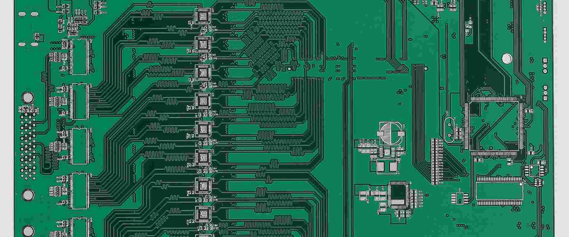
Factors Affecting Impedance
The impedance of a PCB trace is influenced by several factors, including the physical dimensions of the trace, the properties of the dielectric material (substrate), and the presence of nearby conductors or ground planes. Understanding these factors is crucial for accurate impedance calculation and design optimization.
Trace Geometry
The geometry of the PCB trace plays a significant role in determining its impedance. The key parameters that affect impedance include:
- Trace Width (W): The width of the trace directly impacts the impedance. Wider traces generally have lower impedance, while narrower traces have higher impedance.
- Trace Thickness (T): The thickness of the copper trace also influences the impedance. Thicker traces tend to have lower impedance compared to thinner traces.
- Dielectric Thickness (H): The thickness of the dielectric material (substrate) between the trace and the reference plane (ground plane or power plane) is a critical factor in impedance calculation. Increasing the dielectric thickness generally increases the impedance.
Dielectric Properties
The properties of the dielectric material (substrate) used in the PCB construction significantly impact the impedance calculation. The key parameters to consider are:
- Dielectric Constant (Er): The dielectric constant, also known as relative permittivity, is a measure of the material’s ability to store electrical energy. Materials with higher dielectric constants generally result in lower impedance.
- Loss Tangent (tan δ): The loss tangent represents the dielectric material’s energy dissipation characteristics. It is related to the signal attenuation and should be minimized for high-frequency applications.
Presence of Reference Planes
The presence and proximity of reference planes (ground planes or power planes) also influence the impedance of a PCB trace. These planes act as return paths for the signal currents and affect the capacitance and inductance of the transmission line.
- Ground Plane: The distance between the trace and the ground plane (dielectric thickness) impacts the impedance. Closer ground planes generally result in lower impedance.
- Power Plane: Similarly, the presence of a power plane in close proximity to the trace can affect the impedance calculation.
Adjacent Traces and Coupling
In dense PCB layouts, the impedance of a trace can be influenced by the presence of adjacent traces due to electromagnetic coupling effects. The spacing between traces and their relative positions can affect the impedance and introduce crosstalk or other signal integrity issues.
Impedance Calculation Methods
There are several methods for calculating the impedance of PCB traces, each with its own advantages and limitations. The choice of method depends on the specific design requirements, the desired level of accuracy, and the available tools or resources.
Analytical Formulas
Analytical formulas provide closed-form expressions for calculating the impedance of PCB traces based on their physical dimensions and material properties. These formulas are derived from electromagnetic theory and make certain assumptions or approximations.
Microstrip Line Impedance
For microstrip lines, where the trace is on the outer layer of the PCB and the reference plane is on the opposite side of the dielectric, a widely used formula is:Copy code
Z0 = (87 / sqrt(Er + 1.41)) * ln(5.98 * H / (0.8 * W + T))
Where:
- Z0 is the characteristic impedance (ohms)
- Er is the relative permittivity (dielectric constant) of the substrate
- H is the dielectric thickness (height between the trace and the reference plane)
- W is the trace width
- T is the trace thickness
This formula is accurate for a wide range of geometries and dielectric constants but assumes an infinitely thin trace and a single reference plane.
Stripline Impedance
For stripline configurations, where the trace is embedded between two reference planes, the following formula can be used:Copy code
Z0 = (60 / sqrt(Er)) * ln(4 * H / (0.67 * pi * (0.8 * W + T)))
Where the variables have the same meanings as in the microstrip line formula.
These analytical formulas provide a good starting point for impedance calculations and can be used in preliminary design stages or when rough estimates are sufficient.
Numerical Simulations
For more accurate impedance calculations, especially in complex geometries or when considering coupling effects, numerical simulations are often employed. These simulations rely on computational electromagnetic (CEM) techniques, such as the finite element method (FEM) or the method of moments (MoM), to solve Maxwell’s equations and calculate the impedance.
Numerical simulations can account for various factors, including:
- Non-rectangular trace geometries
- Multiple reference planes or power planes
- Dielectric material anisotropy and non-homogeneity
- Coupling between adjacent traces or vias
- Skin effect and conductor roughness
While numerical simulations provide highly accurate results, they require specialized software tools and can be computationally intensive, especially for large or complex designs.
Impedance Calculators and Online Tools
Several online tools and calculators are available for quickly estimating the impedance of PCB traces based on user-provided parameters. These tools typically implement analytical formulas or simplified numerical models and can be useful for quick checks or preliminary designs.
However, it’s important to note that these online tools may have limitations or make certain assumptions, and their accuracy should be verified against more rigorous simulation or measurement methods for critical designs.
Experimental Measurements
In some cases, especially for high-frequency or critical designs, experimental measurements may be necessary to validate the calculated impedance values or to account for manufacturing variations and other real-world factors.
Techniques such as time-domain reflectometry (TDR) or vector network analyzer (VNA) measurements can be used to directly measure the impedance of PCB traces or transmission lines. These methods provide accurate impedance profiles over a wide frequency range but require specialized equipment and expertise.
Design Considerations and Optimization
Calculating the impedance of PCB traces is just the first step in ensuring signal integrity and optimal performance. Several design considerations and optimization techniques should be employed to ensure proper impedance control and minimize signal degradation.
Trace Routing and Layout
Proper trace routing and layout are crucial for maintaining consistent impedance and minimizing reflections and crosstalk. Some best practices include:
- Maintaining consistent trace widths and spacing throughout the signal path
- Avoiding abrupt changes in trace geometry or dielectric thickness
- Minimizing trace lengths and reducing stubs or discontinuities
- Careful placement of vias and consideration of via stubs
- Maintaining adequate spacing between traces to reduce coupling effects
Impedance Matching
To minimize reflections and ensure efficient signal transmission, it is essential to match the impedance of the PCB traces to the impedance of the source and load components. This can be achieved through careful component selection or by using impedance matching techniques, such as series or parallel termination resistors.
Differential Signaling
For high-speed or noise-sensitive applications, differential signaling can be employed to improve signal integrity and reduce electromagnetic interference (EMI). In differential signaling, two complementary signals are transmitted on a pair of traces with tightly controlled impedance and spacing.
Calculating the differential impedance and ensuring matched lengths and coupling between the trace pairs is crucial for maintaining signal quality and common-mode rejection.
Stackup Design and Material Selection
The design of the PCB stackup, including the layer arrangement, dielectric materials, and reference plane configurations, plays a significant role in impedance control. Careful selection of dielectric materials with appropriate dielectric constants and loss characteristics can optimize signal transmission and minimize signal degradation.
Impedance Optimization Techniques
In addition to the design considerations mentioned above, several optimization techniques can be employed to achieve desired impedance values or minimize impedance variations across the PCB.
Trace Width Adjustment
One of the most common techniques for impedance optimization is adjusting the trace width. Wider traces generally have lower impedance, while narrower traces have higher impedance. By selectively modifying the trace widths, designers can fine-tune the impedance to meet target values or match impedances across different signal paths.
Dielectric Thickness Adjustment
Changing the dielectric thickness between the trace and the reference plane can also be used to optimize impedance. Increasing the dielectric thickness generally increases the impedance, while decreasing it lowers the impedance. This technique is particularly useful when working with multi-layer PCBs and when trace width adjustments are limited by design rules or space constraints.
Embedded Components and Embedded Capacitance
In some cases, embedding components or introducing controlled capacitance can be used to adjust the impedance of PCB traces. This approach is often employed in high-frequency or RF designs, where precise impedance control is critical. However, it requires careful simulation and validation to ensure proper impedance matching and signal integrity.
Impedance Profiling and Compensation
For complex designs or high-speed applications, it may be necessary to measure and profile the impedance along the entire signal path. This can be done using time-domain reflectometry (TDR) or vector network analyzer (VNA) measurements. Once the impedance profile is obtained, appropriate compensation techniques, such as trace geometry adjustments or the use of impedance-compensating components, can be employed to minimize impedance variations and ensure consistent signal integrity.
Practical Examples and Case Studies
To further illustrate the concepts and methods discussed in this article, let’s consider a few practical examples and case studies.
Example 1: Microstrip Line Impedance Calculation
Suppose we have a microstrip line on an FR-4 substrate (dielectric constant Er = 4.4) with the following parameters:
- Trace width (W) = 0.2 mm
- Trace thickness (T) = 0.035 mm
- Dielectric thickness (H) = 0.3 mm
Using the microstrip line impedance formula:Copy code
Z0 = (87 / sqrt(Er + 1.41)) * ln(5.98 * H / (0.8 * W + T)) = (87 / sqrt(4.4 + 1.41)) * ln(5.98 * 0.3 / (0.8 * 0.2 + 0.035)) = 50.3 ohms
This example demonstrates how the physical dimensions and dielectric properties can be used to calculate the impedance of a microstrip line using an analytical formula.
Example 2: Stripline Impedance Calculation
Consider a stripline configuration with the following parameters:
- Trace width (W) = 0.15 mm
- Trace thickness (T) = 0.025 mm
- Dielectric thickness (H) = 0.2 mm
- Dielectric constant (Er) = 3.8
Using the stripline impedance formula:Copy code
Z0 = (60 / sqrt(Er)) * ln(4 * H / (0.67 * pi * (0.8 * W + T))) = (60 / sqrt(3.8)) * ln(4 * 0.2 / (0.67 * pi * (0.8 * 0.15 + 0.025))) = 52.1 ohms
This example illustrates the calculation of impedance for a stripline configuration, which is commonly used in multi-layer PCBs or when shielding is required.
Case Study: Impedance Optimization for High-Speed Serial Link
In this case study, we will explore the process of impedance optimization for a high-speed serial link operating at 10 Gbps. The design requirements specify a target impedance of 50 ohms with a tolerance of ±10%.
The initial design uses a microstrip line on an FR-4 substrate with the following parameters:
- Trace width (W) = 0.25 mm
- Trace thickness (T) = 0.035 mm
- Dielectric thickness (H) = 0.3 mm
- Dielectric constant (Er) = 4.4
Using the microstrip line impedance formula, the initial impedance is calculated to be:Copy code
Z0 = (87 / sqrt(Er + 1.41)) * ln(5.98 * H / (0.8 * W + T)) = (87 / sqrt(4.4 + 1.41)) * ln(5.98 * 0.3 / (0.8 * 0.25 + 0.035)) = 45.7 ohms
This initial impedance value falls outside the specified tolerance range of 45 to 55 ohms.
To optimize the impedance, we can employ the following techniques:
- Trace Width Adjustment: By increasing the trace width to 0.3 mm, the impedance becomes:
Copy code
Z0 = (87 / sqrt(4.4 + 1.41)) * ln(5.98 * 0.3 / (0.8 * 0.3 + 0.035)) = 49.2 ohms
This value falls within the desired tolerance range.
- Dielectric Thickness Adjustment: Alternatively, if trace width adjustment is not feasible due to design rules or space constraints, we can adjust the dielectric thickness. By increasing the dielectric thickness to 0.35 mm, the impedance becomes:
Copy code
Z0 = (87 / sqrt(4.4 + 1.41)) * ln(5.98 * 0.35 / (0.8 * 0.25 + 0.035)) = 51.1 ohms
This value also falls within the desired tolerance range.
- Combination of Adjustments: In some cases, a combination of trace width and dielectric thickness adjustments may be required to achieve the desired impedance value.
After implementing the chosen optimization technique(s), it is recommended to perform simulations or experimental measurements to validate the impedance and ensure signal integrity across the entire operating frequency range.
Frequently Asked Questions (FAQs)
- What is the difference between characteristic impedance and differential impedance?
Characteristic impedance refers to the impedance of a single trace or transmission line, while differential impedance refers to the impedance between a pair of traces used for differential signaling. Differential impedance is typically lower than the characteristic impedance of a single trace and is crucial for maintaining signal quality and common-mode rejection in differential signaling systems.
- How does the presence of adjacent traces affect impedance?
Adjacent traces can introduce coupling effects that influence the impedance of a PCB trace. Electromagnetic coupling between traces can change the effective capacitance and inductance, resulting in impedance variations. Proper spacing and shielding techniques are essential to minimize these coupling effects and maintain consistent impedance.
- What is the impact of vias on impedance?
Vias, which are used to transition signals between layers in a multi-layer PCB, can introduce discontinuities and impedance mismatches.


Leave a Reply