Table of Contents
- Introduction to PCB Fabrication
- Materials and Tools Required
- Designing Your PCB
- Toner Transfer Method
- Step 1: Printing the PCB Design
- Step 2: Preparing the Copper Board
- Step 3: Transferring the Toner
- Step 4: Etching the PCB
- Step 5: Cleaning and Drilling
- UV Exposure Method
- Step 1: Printing the PCB Design on Transparency
- Step 2: Preparing the Photoresist-Coated Copper Board
- Step 3: Exposing the PCB
- Step 4: Developing the PCB
- Step 5: Etching the PCB
- Step 6: Cleaning and Drilling
- FAQ
- Conclusion
Introduction to PCB Fabrication
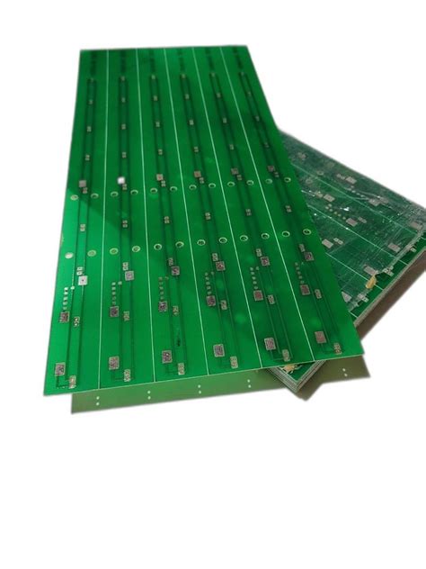
Printed Circuit Boards (PCBs) are the backbone of modern electronics. They provide a way to mechanically support and electrically connect electronic components using conductive tracks, pads, and other features etched from copper sheets laminated onto a non-conductive substrate. PCB fabrication is the process of creating these boards, which can be done professionally or at home using various methods.
Homemade PCB fabrication offers several advantages, such as cost savings, quick turnaround times, and the ability to create custom designs for personal projects. In this article, we will focus on two popular methods for making PCBs at home: the toner transfer method and the UV exposure method.

Materials and Tools Required
Before we dive into the step-by-step instructions for each method, let’s take a look at the materials and tools you’ll need:
| Material/Tool | Toner Transfer Method | UV Exposure Method |
|---|---|---|
| PCB design software | ✓ | ✓ |
| Laser printer | ✓ | ✓ |
| Glossy photo paper or magazine paper | ✓ | |
| Transparency film | ✓ | |
| Copper-clad board | ✓ | |
| Photoresist-coated copper board | ✓ | |
| Clothes iron | ✓ | |
| UV exposure unit | ✓ | |
| Developing solution | ✓ | |
| Etching solution (ferric chloride or hydrochloric acid/hydrogen peroxide) | ✓ | ✓ |
| Plastic container for etching | ✓ | ✓ |
| Rubber gloves and safety goggles | ✓ | ✓ |
| Acetone or isopropyl alcohol | ✓ | ✓ |
| Drill or Dremel tool | ✓ | ✓ |

Designing Your PCB
Before you can start fabricating your PCB, you need to design it using PCB design software. There are many options available, both free and paid, such as KiCad, Eagle, and Altium Designer. When designing your PCB, keep in mind the following tips:
- Use a grid to ensure proper component placement and routing
- Follow the manufacturer’s guidelines for minimum trace width and spacing
- Include mounting holes and a ground plane if necessary
- Double-check your design for errors before proceeding to fabrication
Once you have completed your PCB design, export it as a PDF or image file for printing.

Toner Transfer Method
The toner transfer method is a popular and affordable way to make PCBs at home. It involves printing your PCB design onto glossy paper using a laser printer, then transferring the toner onto a copper-clad board using heat.
Step 1: Printing the PCB Design
- Load glossy photo paper or magazine paper into your laser printer.
- Print your PCB design onto the glossy side of the paper, making sure the design is mirrored (flipped horizontally).
- Cut out the printed design, leaving a small margin around the edges.
Step 2: Preparing the Copper Board
- Cut your copper-clad board to the appropriate size for your design.
- Clean the copper surface thoroughly with acetone or isopropyl alcohol to remove any dirt or grease.
- Roughen the surface slightly with fine-grit sandpaper to improve toner adhesion.
Step 3: Transferring the Toner
- Place the printed design face-down onto the copper board, aligning it with the edges.
- Use a clothes iron set to its highest setting (without steam) to apply heat and pressure to the back of the paper.
- Press firmly and evenly for several minutes, ensuring the entire design is transferred.
- Allow the board to cool before carefully peeling off the paper.
Step 4: Etching the PCB
- Prepare your etching solution according to the manufacturer’s instructions (ferric chloride or hydrochloric acid/hydrogen peroxide).
- Wearing rubber gloves and safety goggles, place the PCB into the etching solution.
- Agitate the solution gently and monitor the etching process, which may take 15-30 minutes.
- Remove the PCB from the solution once all exposed copper has been etched away.
Step 5: Cleaning and Drilling
- Rinse the etched PCB thoroughly with water and dry it with a clean cloth.
- Remove the remaining toner using acetone or isopropyl alcohol.
- Drill any necessary holes for component leads and mounting using a drill or Dremel tool.
UV Exposure Method
The UV exposure method is another popular way to make PCBs at home, offering higher precision and resolution than the toner transfer method. It involves using a photoresist-coated copper board and exposing it to UV light through a transparency printed with your PCB design.
Step 1: Printing the PCB Design on Transparency
- Load a transparency film into your laser printer.
- Print your PCB design onto the transparency, ensuring the design is mirrored (flipped horizontally).
- Cut out the printed design, leaving a small margin around the edges.
Step 2: Preparing the Photoresist-Coated Copper Board
- Cut your photoresist-coated copper board to the appropriate size for your design.
- Remove the protective film from the photoresist surface.
Step 3: Exposing the PCB
- Place the transparency with the printed design onto the photoresist surface, aligning it with the edges.
- Secure the transparency using clear glass or acrylic to ensure tight contact with the photoresist.
- Expose the board to UV light using a UV exposure unit for the recommended time (usually 2-5 minutes).
Step 4: Developing the PCB
- Prepare the developing solution according to the manufacturer’s instructions.
- Immerse the exposed PCB in the developing solution and agitate gently for 1-2 minutes.
- Remove the PCB from the solution and rinse it thoroughly with water.
Step 5: Etching the PCB
- Prepare your etching solution according to the manufacturer’s instructions (ferric chloride or hydrochloric acid/hydrogen peroxide).
- Wearing rubber gloves and safety goggles, place the developed PCB into the etching solution.
- Agitate the solution gently and monitor the etching process, which may take 15-30 minutes.
- Remove the PCB from the solution once all exposed copper has been etched away.
Step 6: Cleaning and Drilling
- Rinse the etched PCB thoroughly with water and dry it with a clean cloth.
- Remove the remaining photoresist using acetone or isopropyl alcohol.
- Drill any necessary holes for component leads and mounting using a drill or Dremel tool.
FAQ
-
Q: Which method is better for making PCBs at home, toner transfer or UV exposure?
A: Both methods have their advantages. The toner transfer method is more affordable and accessible, while the UV exposure method offers higher precision and resolution. The choice ultimately depends on your specific needs and available resources. -
Q: Can I use an inkjet printer instead of a laser printer for these methods?
A: No, inkjet printers are not suitable for PCB fabrication as the ink does not transfer well to the copper surface. Laser printers use toner, which is a dry powder that adheres to the copper when heated. -
Q: What safety precautions should I take when working with etching solutions?
A: Always wear rubber gloves and safety goggles when handling etching solutions. Work in a well-ventilated area and avoid inhaling fumes. Dispose of used etching solutions according to local regulations. -
Q: Can I make double-sided PCBs using these methods?
A: Yes, both methods can be used to create double-sided PCBs. However, the process is more complex and requires careful alignment of the designs on both sides of the board. -
Q: What can I do if my PCB design doesn’t transfer or develop properly?
A: There are several factors that can affect the success of your PCB fabrication. Ensure that your printer settings are correct, the copper surface is clean and roughened, and the exposure and developing times are appropriate for your specific materials. If issues persist, try adjusting these variables or consult online resources for troubleshooting tips.
Conclusion
Making your own PCBs at home is a rewarding and cost-effective way to bring your electronics projects to life. By following the step-by-step instructions for either the toner transfer method or the UV exposure method, you can create custom PCBs with relative ease. Remember to prioritize safety when working with etching solutions and to take your time when designing and fabricating your boards. With practice and patience, you’ll be able to produce high-quality PCBs for all your projects.
As you explore the world of homemade PCB fabrication, don’t hesitate to experiment with different materials and techniques to find what works best for you. There is a wealth of resources available online, including forums, tutorials, and videos, to help you refine your skills and troubleshoot any issues you may encounter. Happy PCB making!


Leave a Reply