Introduction to DIY PCB
Printed Circuit Boards (PCBs) are the backbone of modern electronic devices. From smartphones to industrial control systems, PCBs provide a reliable and efficient way to connect electronic components. While commercially manufactured PCBs are readily available, creating your own PCB can be a rewarding and educational experience for beginners in electronics. In this article, we will guide you through the process of making a homemade PCB, including the tools and materials needed, design considerations, and step-by-step instructions.
Benefits of Making Your Own PCB
- Cost-effective for small-scale projects
- Customizable to your specific needs
- Enhances understanding of electronic circuits
- Provides a sense of accomplishment

Tools and Materials Required
To create your own PCB, you will need the following tools and materials:
| Tool/Material | Purpose |
|---|---|
| PCB design software | For designing the PCB layout |
| Copper-clad board | The base material for the PCB |
| Laser printer | For printing the PCB design onto transfer paper |
| Transfer paper | To transfer the design onto the copper-clad board |
| Clothes iron | For transferring the design from the paper to the board |
| Ferric chloride solution | For etching the copper-clad board |
| Plastic container | For holding the etching solution |
| Protective gloves and eyewear | For safety during the etching process |
| Drill or Dremel tool | For drilling holes in the PCB |
| Soldering iron and solder | For soldering components onto the PCB |
Choosing the Right PCB Design Software
There are several PCB design software options available, ranging from free open-source tools to commercial software. Some popular choices for beginners include:
- KiCad (open-source)
- EasyEDA (free web-based)
- Fritzing (beginner-friendly)
- Eagle (commercial, free for small boards)
Consider factors such as ease of use, community support, and feature set when selecting the software that best suits your needs.

Designing Your PCB
Creating the Schematic
The first step in designing your PCB is to create a schematic diagram of your electronic circuit. This diagram represents the connections between components using symbols and lines. Follow these steps to create your schematic:
- Open your chosen PCB design software.
- Place the required component symbols on the schematic canvas.
- Connect the components using wires or nets according to your circuit design.
- Assign unique identifiers to each component (e.g., R1 for a resistor, C1 for a capacitor).
- Double-check your connections and ensure the schematic matches your intended design.
Converting Schematic to PCB Layout
Once your schematic is complete, you can convert it into a PCB layout. The PCB layout represents the physical arrangement of components and traces on the copper-clad board. Follow these steps to create your PCB layout:
- Switch to the PCB layout editor in your design software.
- Define the board dimensions and shape.
- Place the component footprints on the board, ensuring proper spacing and orientation.
- Route the traces between the component pads according to your schematic connections.
- Ensure the traces have appropriate width and clearance to avoid short circuits and manufacturing issues.
- Add any necessary text labels, logos, or identifiers to the PCB.
Design Considerations
When designing your PCB, keep the following considerations in mind:
- Component placement: Arrange components in a logical and efficient manner to minimize trace lengths and crossovers.
- Trace width: Use appropriate trace widths based on the current carrying requirements of your circuit.
- Clearance: Maintain sufficient clearance between traces and components to prevent short circuits.
- Ground plane: Consider adding a ground plane to your PCB for better noise reduction and signal integrity.
- Solder mask: Apply a solder mask layer to protect the copper traces from oxidation and accidental short circuits.

Transferring the Design to the Copper-Clad Board
Printing the PCB Design
Once your PCB layout is finalized, you need to transfer the design onto the copper-clad board. Follow these steps:
- Print the PCB design onto a transfer paper using a laser printer. Ensure the print is mirror-imaged.
- Cut the printed design to the size of your copper-clad board.
- Clean the copper-clad board with fine sandpaper or steel wool to remove any oxidation.
- Place the transfer paper onto the copper side of the board, with the printed side facing down.
- Use a clothes iron set to high heat (no steam) to press the paper onto the board for several minutes.
- Allow the board to cool, then carefully peel off the transfer paper. The toner from the printer should have transferred onto the copper surface.
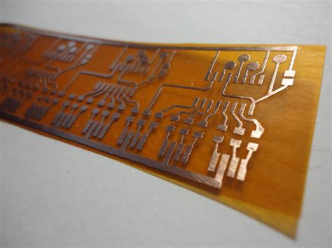
Etching the PCB
With the design transferred onto the copper-clad board, you can now etch away the unwanted copper using a ferric chloride solution. Follow these steps:
- Wear protective gloves and eyewear.
- Pour the ferric chloride solution into a plastic container.
- Immerse the PCB into the solution, with the copper side facing up.
- Agitate the container gently to ensure even etching.
- Monitor the etching process closely. It usually takes around 15-30 minutes for the unwanted copper to dissolve completely.
- Once etching is complete, remove the PCB from the solution and rinse it thoroughly with water.
- Clean the remaining toner from the PCB using acetone or a dedicated PCB cleaner.
Drilling and Soldering
Drilling Holes
After etching, you need to drill holes in the PCB for component leads and mounting. Follow these steps:
- Use a drill or Dremel tool with a suitable bit size for your component leads.
- Carefully drill holes at the marked locations on the PCB.
- Ensure the holes are perpendicular to the board surface to avoid damaging the pads.
Soldering Components
With the holes drilled, you can now solder the components onto the PCB. Follow these steps:
- Insert the component leads through the corresponding holes on the PCB.
- Bend the leads slightly to hold the components in place.
- Heat the soldering iron and apply a small amount of solder to the tip.
- Touch the soldering iron to the component lead and pad simultaneously, allowing the solder to flow and create a joint.
- Repeat the process for all components and leads.
- Trim any excess leads using wire cutters.
Testing and Troubleshooting
After soldering, it’s essential to test your PCB for proper functionality and troubleshoot any issues that may arise. Follow these steps:
- Visually inspect the PCB for any soldering defects, short circuits, or missing components.
- Use a multimeter to check for continuity between the appropriate pads and component leads.
- Power up the PCB and verify its operation using test equipment or by observing expected behaviors.
- If issues are found, refer to the schematic and PCB layout to identify potential problems.
- Rework any soldering issues or replace faulty components as needed.
Frequently Asked Questions (FAQ)
- Can I use any printer for transferring the PCB design?
-
It’s recommended to use a laser printer for transferring the PCB design onto the transfer paper. Inkjet printers may not provide the necessary toner density for a successful transfer.
-
How long does the etching process take?
-
The etching process typically takes around 15-30 minutes, depending on the strength of the ferric chloride solution and the size of your PCB. It’s important to monitor the process closely to avoid over-etching.
-
Can I reuse the ferric chloride solution?
-
Yes, you can reuse the ferric chloride solution for multiple etching sessions. However, the solution will gradually lose its effectiveness over time and may need to be replaced when etching takes significantly longer or becomes inconsistent.
-
What should I do if I encounter soldering difficulties?
-
If you face soldering issues, ensure your soldering iron is at the correct temperature and that you are using the appropriate solder wire gauge. Practice soldering on scrap boards or components to improve your technique. If necessary, seek guidance from experienced electronics enthusiasts or tutorials.
-
How can I improve the quality of my homemade PCBs?
- To enhance the quality of your homemade PCBs, consider the following tips:
- Use high-quality materials, such as clean copper-clad boards and fresh etching solutions.
- Ensure proper cleaning and preparation of the copper surface before transferring the design.
- Maintain consistent temperature and pressure when using the clothes iron for transferring the design.
- Practice proper soldering techniques and use appropriate tools and materials.
- Continuously refine your PCB design skills by studying best practices and experimenting with different layouts.
Conclusion
Creating your own homemade PCB can be a fun and rewarding experience for beginners in electronics. By following the steps outlined in this article, you can design, etch, and assemble a functional PCB using readily available tools and materials. Remember to prioritize safety, practice patience, and learn from any mistakes along the way. As you gain experience and confidence, you can take on more complex projects and explore advanced PCB design techniques. Happy PCB making!


Leave a Reply