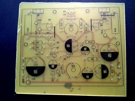
What is a PCB?
A printed circuit board (PCB) is a flat board made of insulating material, such as fiberglass or plastic, with conductive copper traces printed on its surface. These traces connect various electronic components, like resistors, capacitors, and integrated circuits, to form a functional electronic circuit.
PCBs are used in almost all electronic devices, from simple hobby projects to complex industrial equipment. They provide a reliable and efficient way to connect components and ensure proper functioning of the circuit.
Why Make PCBs at Home?
There are several reasons why you might want to make PCBs at home:
-
Cost-effective: Making your own PCBs can be more affordable than ordering them from a manufacturer, especially for small quantities or prototype designs.
-
Customization: When you make your own PCBs, you have complete control over the design and can customize it to fit your specific needs.
-
Learning experience: Creating PCBs at home is an excellent way to learn about electronics and gain hands-on experience with the process.
-
Faster turnaround: By making PCBs at home, you can avoid the wait times associated with ordering from a manufacturer, allowing you to test and iterate on your designs more quickly.

Materials and Tools Required
Before we dive into the process of making PCBs, let’s review the materials and tools you’ll need:
| Material/Tool | Description |
|---|---|
| PCB blank | Copper-clad board with a substrate material like fiberglass or FR-4 |
| PCB design software | Software to create and edit PCB layouts (e.g., KiCad, Eagle) |
| Laser printer | Used to print the PCB design onto a transfer paper |
| Transfer paper | Special paper that transfers the printed design onto the PCB |
| Clothes iron | Used to transfer the design from the paper to the PCB |
| Etching solution | Chemical solution (e.g., ferric chloride) to remove unwanted copper |
| Plastic container | Used to hold the etching solution during the etching process |
| Drill or drill press | Used to drill holes for component leads and mounting |
| Safety equipment | Gloves, goggles, and a well-ventilated work area |

Step-by-Step Guide to Making PCBs at Home
Step 1: Design Your PCB
The first step in making a PCB is to design the circuit using PCB design software. There are many free and paid options available, such as KiCad and Eagle. These programs allow you to create a schematic of your circuit and then convert it into a PCB layout.
When designing your PCB, consider factors like component placement, trace width, and spacing between traces to ensure proper functionality and manufacturability.
Step 2: Print the PCB Design
Once your PCB design is complete, print it onto a special transfer paper using a laser printer. Make sure to print the design in mirror image, as it will be transferred onto the copper side of the PCB.
Step 3: Transfer the Design to the PCB
Place the printed transfer paper onto the copper side of the PCB blank, with the printed side facing down. Use a clothes iron set to high heat (without steam) to transfer the design onto the copper. Apply even pressure and heat for several minutes, ensuring that the entire design is transferred.
After ironing, let the PCB cool down and then carefully peel off the transfer paper. The design should now be visible on the copper surface.
Step 4: Etch the PCB
Prepare your etching solution according to the manufacturer’s instructions. Typically, this involves diluting the concentrated solution with water in a plastic container.
Submerge your PCB in the etching solution, with the copper side facing up. Agitate the container gently to ensure even etching. The etching process can take anywhere from 10 to 45 minutes, depending on the strength of the solution and the size of your PCB.
Monitor the etching process closely. Once all the unwanted copper has been removed, leaving only your circuit traces, remove the PCB from the solution and rinse it thoroughly with water.
Step 5: Drill Holes and Clean the PCB
Using a drill or drill press, carefully drill holes at the locations marked in your PCB design for component leads and mounting holes.
After drilling, clean the PCB with steel wool or fine sandpaper to remove any remaining resist or oxidation from the copper traces. This will ensure better solderability.
Step 6: Solder Components
Finally, solder your electronic components onto the PCB according to your circuit design. Make sure to use a high-quality soldering iron and solder, and follow proper soldering techniques to ensure strong and reliable connections.

Tips and Tricks for Successful PCB Making
- Always wear safety gear and work in a well-ventilated area when handling chemicals like etching solution.
- Double-check your PCB design before printing to avoid costly mistakes.
- Use high-quality materials, such as fresh etching solution and clean copper-clad boards, for best results.
- Practice proper soldering techniques to ensure reliable connections and avoid damaging components.
- Start with simple designs and work your way up to more complex circuits as you gain experience.
Frequently Asked Questions (FAQ)
-
Can I use any type of paper for transferring the PCB design?
No, you should use a special transfer paper designed for PCB making. Regular paper will not work effectively and may result in a poor transfer of the design. -
How long does the etching process take?
The etching process can take anywhere from 10 to 45 minutes, depending on factors like the strength of the etching solution, the size of your PCB, and the ambient temperature. -
Can I reuse the etching solution?
Yes, you can reuse the etching solution multiple times. However, keep in mind that the solution will become less effective over time as it dissolves more copper. Dispose of the solution properly when it becomes too weak to etch effectively. -
What should I do if my PCB design doesn’t transfer properly?
If your PCB design doesn’t transfer well, check that you printed the design in mirror image and used the correct type of transfer paper. Ensure that you applied even heat and pressure during the ironing process. If the problem persists, try adjusting your printer settings or using a different transfer paper. -
How can I improve the quality of my homemade PCBs?
To improve the quality of your PCBs, use high-quality materials, follow proper techniques, and practice regularly. Double-check your designs, ensure proper alignment when transferring, and be patient during the etching process. As you gain experience, you’ll be able to create more complex and professional-looking PCBs.
Conclusion
Making PCBs at home is a rewarding and educational experience for electronics enthusiasts. By following this easy approach and using the right materials and tools, you can create custom PCBs for your projects in the comfort of your own home. Remember to prioritize safety, start with simple designs, and practice regularly to improve your skills. Happy PCB making!


Leave a Reply