Introduction to Hex Inverter ICs
A hex inverter IC, also known as a NOT gate or inverting buffer, is a digital logic integrated circuit that performs logical negation on six independent inputs. It takes a binary input signal and inverts it to the opposite state at the output. For example, if the input is a logical high (1), the output will be a logical low (0), and vice versa.
Hex inverters are widely used in various digital circuits and systems for signal conditioning, level shifting, and implementing basic logic functions. They are essential building blocks in many electronic applications, such as:
- Digital logic circuits
- Microprocessor systems
- Memory devices
- Interfacing between different logic families
- Waveform generation
- Pulse shaping and conditioning
How Hex Inverters Work
A hex inverter IC contains six independent inverter gates, each performing the NOT operation on its respective input. The inverter gate is the simplest form of a logic gate, consisting of a single input and a single output. The output state is always the opposite of the input state.
Internally, each inverter gate is typically implemented using two complementary metal-oxide-semiconductor (CMOS) transistors: an n-channel MOSFET (NMOS) and a p-channel MOSFET (PMOS). The NMOS and PMOS transistors are connected in series between the power supply (VCC) and ground (GND).
When the input is low (0), the PMOS transistor is turned on, and the NMOS transistor is turned off. This connects the output to VCC, resulting in a high (1) output state. Conversely, when the input is high (1), the PMOS transistor is turned off, and the NMOS transistor is turned on, connecting the output to GND and resulting in a low (0) output state.
The truth table for a single inverter gate is as follows:
| Input | Output |
|---|---|
| 0 | 1 |
| 1 | 0 |
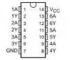
Hex Inverter IC Pinout and Packaging
Hex inverter ICs are commonly available in various package types, such as dual in-line package (DIP), small outline integrated circuit (SOIC), and thin shrink small outline package (TSSOP). The most popular package is the 14-pin DIP, which has the following pinout:
| Pin | Function |
|---|---|
| 1 | Input A |
| 2 | Output Y |
| 3 | Input B |
| 4 | Output Y |
| 5 | Input C |
| 6 | Output Y |
| 7 | GND |
| 8 | Output Y |
| 9 | Input D |
| 10 | Output Y |
| 11 | Input E |
| 12 | Output Y |
| 13 | Input F |
| 14 | VCC |
The IC has six inverter gates, each with its own input (A, B, C, D, E, F) and output (Y). The VCC pin is connected to the positive power supply, typically +5V, while the GND pin is connected to the ground or negative power supply.
Popular Hex Inverter IC Series
There are several popular hex inverter IC series, each with its own characteristics and specifications. Some of the most common series include:
1. 7404 Series
The 7404 series is a popular choice for general-purpose inverter applications. It is part of the 74xx family of TTL (Transistor-Transistor Logic) devices. The 7404 hex inverter operates with a supply voltage of 5V and has a propagation delay of approximately 10 nanoseconds.
2. 74HC04 Series
The 74HC04 series is a high-speed CMOS version of the hex inverter. It offers faster switching speeds and lower power consumption compared to the 7404 series. The 74HC04 operates with a supply voltage range of 2V to 6V and has a propagation delay of around 8 nanoseconds.
3. 74HCT04 Series
The 74HCT04 series is similar to the 74HC04 but is designed to be compatible with TTL input levels. It allows interfacing between CMOS and TTL devices without the need for additional level-shifting circuitry. The 74HCT04 operates with a supply voltage of 5V and has a propagation delay of approximately 9 nanoseconds.
4. 4069UB Series
The 4069UB series is part of the 4000 series of CMOS devices. It is known for its low power consumption and wide supply voltage range (3V to 15V). The 4069UB hex inverter has a slower switching speed compared to the 74xx series, with a propagation delay of around 50 nanoseconds at 5V supply voltage.

Applications of Hex Inverters
Hex inverters find numerous applications in digital electronics and logic design. Some common applications include:
1. Signal Inversion
The primary function of a hex inverter is to invert the polarity of a digital signal. It is used when a signal needs to be inverted to meet the requirements of subsequent stages or to maintain the correct logic levels in a circuit.
2. Level Shifting
Hex inverters can be used for level shifting between different logic families or voltage levels. By connecting the input to one logic level and the output to another, the inverter acts as a simple level translator. This is particularly useful when interfacing devices with different operating voltages.
3. Waveform Generation
Hex inverters can be configured as oscillators or astable multivibrators to generate square wave or rectangular waveforms. By connecting the output of one inverter to the input of another and adding appropriate timing components (resistors and capacitors), various waveforms with different frequencies can be generated.
4. Pulse Conditioning
Inverters can be used to condition digital pulses by sharpening the edges, removing noise, or adjusting the pulse width. By cascading multiple inverters in series, the rise and fall times of the pulses can be improved, resulting in cleaner and more reliable digital signals.
5. Implementing Logic Functions
Hex inverters can be combined with other logic gates to implement various logic functions. By using inverters in conjunction with AND, OR, NAND, or NOR gates, complex combinational and sequential logic circuits can be designed.

Interfacing with Hex Inverters
When interfacing with hex inverters, there are a few considerations to keep in mind:
1. Input and Output Voltage Levels
Ensure that the input voltage levels are compatible with the specific hex inverter IC being used. The input voltage should be within the permissible range specified in the datasheet. Similarly, the output voltage levels will depend on the supply voltage and the logic family of the inverter.
2. Load Capacitance
The output of a hex inverter can drive a certain amount of load capacitance. Exceeding the maximum load capacitance can lead to slower switching speeds and increased propagation delays. Consult the datasheet for the maximum allowable load capacitance and design the circuit accordingly.
3. Unused Inputs
If any of the inverter gates in a hex inverter IC are unused, it is good practice to tie the unused inputs to either VCC or GND. Leaving them floating can result in unstable operation and increased power consumption. Tying unused inputs to a known state ensures proper functioning of the IC.
4. Decoupling Capacitors
When using hex inverters, it is recommended to include decoupling capacitors close to the VCC and GND pins of the IC. Decoupling capacitors help to filter out noise and provide a stable power supply to the device. A typical value for the decoupling capacitor is 0.1μF ceramic capacitor.

Advantages and Disadvantages of Hex Inverters
Hex inverters offer several advantages and have some limitations. Let’s explore them:
Advantages
-
Simplicity: Hex inverters are simple and easy to use. They perform the basic NOT operation and require minimal external components.
-
Versatility: Hex inverters can be used in a wide range of applications, from signal inversion and level shifting to waveform generation and pulse conditioning.
-
Compatibility: Hex inverters are available in various logic families, making them compatible with different voltage levels and logic standards.
-
Low Cost: Hex inverter ICs are relatively inexpensive and readily available, making them cost-effective for many applications.
Disadvantages
-
Limited Functionality: Hex inverters only perform the NOT operation. For more complex logic functions, additional gates or circuits are required.
-
Propagation Delay: Like all digital devices, hex inverters introduce a certain amount of propagation delay. This delay can limit the maximum operating frequency of the circuit.
-
Power Consumption: While CMOS hex inverters are known for their low power consumption, TTL-based inverters may consume more power compared to other logic families.
-
Noise Sensitivity: Hex inverters can be sensitive to noise on the input signals. Proper noise filtering and decoupling techniques should be employed to ensure reliable operation.
Frequently Asked Questions (FAQs)
- What is the difference between a hex inverter and a NOT gate?
A hex inverter and a NOT gate perform the same logical operation, which is inverting the input signal. The main difference is that a hex inverter IC contains six independent inverter gates in a single package, while a NOT gate refers to a single inverter unit.
- Can hex inverters be used with any logic family?
Hex inverters are available in different logic families, such as TTL, CMOS, and their subsets (e.g., HC, HCT). Each logic family has its own operating voltage ranges and input/output characteristics. It is important to choose the appropriate hex inverter IC that is compatible with the logic family being used in the circuit.
- How do I determine the output voltage levels of a hex inverter?
The output voltage levels of a hex inverter depend on the supply voltage (VCC) and the logic family. For example, in the TTL family, a logical high output is typically around 3.5V to 5V, while a logical low output is between 0V and 0.4V. In CMOS devices, the output levels are closer to the supply voltage rails. Refer to the datasheet of the specific hex inverter IC for detailed information on the output voltage levels.
- What happens if I leave an unused input of a hex inverter floating?
Leaving an unused input of a hex inverter floating can lead to unstable operation and increased power consumption. It is recommended to tie unused inputs to either VCC or GND, depending on the desired output state. This ensures that the inverter gate is in a known state and prevents any unwanted behavior.
- Can hex inverters be used for analog signal processing?
Hex inverters are primarily designed for digital signal processing and are not suitable for analog signal processing. They operate with discrete voltage levels (high and low) and do not provide linear amplification or continuous output states. For analog signal processing, operational amplifiers (op-amps) or other linear circuits are more appropriate.
Conclusion
Hex inverter ICs are essential building blocks in digital electronics, providing the basic NOT operation in a compact and convenient package. They find wide applications in signal inversion, level shifting, waveform generation, pulse conditioning, and implementing logic functions.
When working with hex inverters, it is important to consider factors such as input/output voltage levels, load capacitance, unused inputs, and decoupling capacitors. By understanding the characteristics and limitations of hex inverters, designers can effectively incorporate them into their digital circuits and systems.
Whether you are a beginner learning about digital logic or an experienced engineer designing complex systems, hex inverters are valuable tools to have in your electronics toolkit. Their simplicity, versatility, and wide availability make them indispensable in many electronic applications.
As you explore the world of digital electronics, don’t hesitate to experiment with hex inverters and discover their potential in your projects. With a solid understanding of their functionality and proper implementation techniques, you can unleash the power of these tiny but mighty integrated circuits.


Leave a Reply