High density interconnect (HDI) rigid flex PCBs provide several benefits over traditional rigid PCBs or flex PCBs alone. As the name suggests, HDI rigid flex combines the best aspects of both rigid and flex PCB technologies into one advanced circuit board solution.
What are HDI Rigid Flex PCBs?
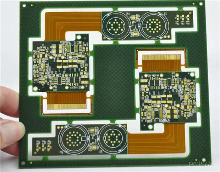
HDI rigid flex PCBs contain both rigid sections and flexible sections joined together in one circuit board. The rigid sections provide structural stability and allow for fine trace routing, while the flexible sections enable the PCB to bend and flex to fit various form factors.
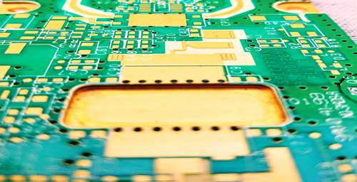
HDI refers to the use of microvias or vias with extremely small diameters (typically under 0.15mm) drilled with laser technology. HDI allows for higher circuit density with more routing channels by enabling trace routes in multiple layers connected through dense stacked microvias.
Some key characteristics of HDI rigid flex PCBs:
- Combines rigid and flex materials into one board
- Uses microvias for increased circuit density
- Enables flexible bending in certain areas
- Maintains rigidity in other sections
- Complex multilayer construction
- May contain components mounted on both rigid and flex regions
- Efficient routing for complex, compact designs
Benefits of HDI Rigid Flex PCBs
1. Ideal for Complex Layouts in Small Spaces
The combination of rigid and flex allows HDI rigid flex PCBs to optimize routing across both rigid and flex sections, facilitating complex layouts in very compact spaces. The rigid portions provide stability for mounting components, while the flex areas enable three-dimensional shaping to fit multi-axis designs.
HDI microvias enable four or more routing layers in the rigid sections, multiplying the available channels for traces. This allows far greater circuit density, accommodating more complex circuits in less space.
2. Reduces Assembly Costs
By integrating rigid and flex materials into one board, HDI rigid flex PCBs eliminate the need to interconnect separate rigid and flex PCBs. The costs associated with connectors, cabling, and assembly labor to interconnect boards are avoided.
HDI rigid flex PCBs also reduce assembly costs by enabling streamlined production. Components can be rapidly surface mounted on both rigid and flex areas using standard SMT equipment.
3. Improves Reliability
With HDI rigid flex PCBs, the connections between the rigid and flex sections are integral to the base board. This results in a more reliable design versus having individual rigid and flex PCBs joined through connectors and cables.
The continual flexion of separate rigid and flex PCBs interconnected by cables strains the solder joints of connectors. In contrast, an HDI rigid flex PCB flexes naturally without stressing connections.
4. Reduces Weight and Volume
HDI rigid flex PCBs occupy significantly less volume than the combination of separate rigid and flex PCBs stacked or joined by cables. This reduces product weight and frees up space for other components.
The thin, tight microvias of HDI technology enable very compact vertical spacing through multiple layers. And the flexibility of the flex regions eliminates the need for extraneous cabling that would otherwise increase volume.
5. Facilitates Advanced Electrical Performance
HDI microvias exhibit lower inductance and resistance than traditional plated through-hole vias, resulting in enhanced high frequency behavior. The dense microvias offer shorter travel distances for signals, minimizing parasitic capacitance for improved electrical performance.
Industries Using HDI Rigid Flex PCBs
HDI rigid flex PCBs support many advanced electronics applications, but are especially prevalent in the following industries:
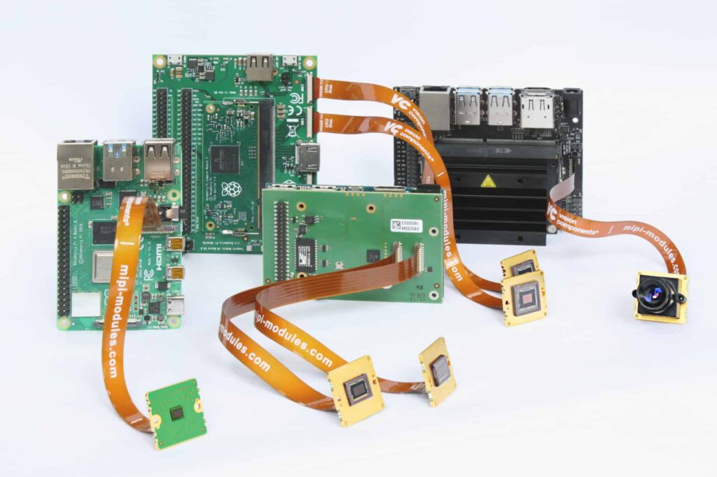
Consumer Electronics
- Cell phones
- Laptops
- Tablets
- Wearables
- IoT devices
Automotive Electronics
- Navigation and infotainment systems
- Advanced driver assistance systems (ADAS)
- EV and hybrid control systems
Medical Electronics
- Implants
- Wearables
- Monitoring devices
Aerospace and Defense
- Avionics
- Radar, guidance, and communication systems
HDI Rigid Flex PCB Design Considerations
Designing an HDI rigid flex PCB requires advanced skills and specialized software tools. Here are some of the important design factors:
Layer Stackup
The designer must strategically build up the layer stackup, selecting the number of layers in rigid vs. flex areas, dielectric materials, and copper weights. This provides the foundation to route traces optimally between layers.
High-Speed Routing
HDI rigid flex PCBs frequently carry high-speed signals demanding impedance control and termination planning. This involves managing trace width/spacing, routing layer pairs, and reference planes.
Component Layout
Both rigid and flex areas have unique requirements for component placement and trace routing that must be addressed. Thermal design for heat dissipation also becomes critical.
Flex-to-Rigid Transition
The intersections between rigid and flex sections require special attention to avoid over-stressing the materials during flexing. Teardrop shapes help prevent cracks from propagating.
Rigid-Flex Registration
Careful registration during board fabrication is essential for ensuring reliable connections between the traced on the separate rigid and flex layers.
Coverlay Opening Design
The flexible coverlay material must be properly cut and opened around surface mount component pads and other interface areas.
Vias
In addition to dense HDI microvias in rigid sections, larger mechanically drilled vias are often used strategically in the flex areas.
HDI Rigid Flex PCB Fabrication
Fabricating HDI rigid flex PCBs requires sophisticated processes, specialized materials, and advanced equipment capable of very tight tolerances and registration. Here is an overview of the fabrication steps:
Imaging
The fabrication starts with lithographic imaging of the traces and features from the CAD data onto photoimageable rigid and flex dielectric layers.
Layer Alignment
The separately imaged rigid and flex layers are carefully aligned and laminated together with bondply layers in between. Registration accuracy is critical.
Microvia Formation
Microvias are drilled through the rigid layers using precise lasers. The small diameters and high density are enabled by laser tolerances under 0.025mm.
Metallization
The layers are treated and metallized to activate catalysts and deposit copper onto the traced circuitry patterns and within the microvias for conductivity.
Outer Layer Imaging
Additional traces, pads, and features are added to the outer rigid and flex layers through lithographic imaging. Flex connectors are often traced on the outer layers.
Component Holes
Larger mechanically drilled holes are created for through-hole component leads and other interconnections between layers.
Solder Mask
A solder mask material is laminated onto the outer board surfaces and imaged to selectively cover untraced areas and expose solderable component pads.
Final Metallization
Final electroless or electrolytic plating deposits more copper to desired thicknesses onto exposed traced areas not covered by solder mask.
Test and Inspection
Each completed HDI rigid flex PCB is electrically tested and inspected for defects with automated optical inspection (AOI) and other techniques.
This multi-stage fabrication process requires high-end capabilities and know-how to reliably produce quality HDI rigid flex PCBs.
Key HDI Rigid Flex PCB Materials
HDI rigid flex PCBs integrate a number of specialized materials optimized for their purposes. Some key materials include:
- Rigid laminates – FR-4, polyimide, PTFE, ceramic-filled epoxy
- Flexible laminates – Polyimide, PEN, PET, polymide
- Bondply layers – Adhesive-coated materials that bond the rigid and flex layers
- Coverlay – Flexible solder mask material
- Copper foils – Rolled copper of varying weights measured in ounces per square foot
Rigid and flexible laminate materials are chosen based on dielectric properties, thermal tolerance, and other factors suited to the application.
HDI Rigid Flex PCB Design Software
To effectively design HDI rigid flex PCBs, PCB designers need software tools capable of addressing their unique demands. Key capabilities include:
- Importing rigid and flex CAD data
- Layer stackup design
- Split power plane layers
- Rigid-flex transition modeling
- Flex-to-rigid component placement tools
- Microvia and padstack integration
- High-speed routing with length tuning
- 3D modeling of flex bending
- Automated coverlay cutouts
- Design rule checking (DRC) tools
- Thermal analysis simulation
- Data preparation for accurate layer-to-layer registration
Leading HDI rigid flex design solutions include Mentor Xpedition, Cadence Allegro, and Altium Designer. These provide extensive toolsets tailored specifically for the needs of rigid flex PCB design.
HDI Rigid Flex PCB Testing
Verifying the performance of complex HDI rigid flex PCBs requires thorough testing. Some key testing methods include:
Electrical Testing – Tests for continuity, resistance, capacitance, and high-speed signal integrity using fixtures that access testpoints on the board.
ICT – In-circuit test systems verify proper connections between components mounted on the assembled board.
Flying Probe – For assemblies not suited for fixture-based testing, flying probe testers make electrical measurements by lowering probes onto pads.
Automated Optical Inspection – Optical inspection systems check assembly quality, identifying defects like missing or misaligned components.
Flex Cycle Testing – Subjects boards and assemblies to repeated bending cycles and then tests for electrical continuity failures caused by flex stress.
X-Ray Imaging – X-ray images enable inspecting the internal structure, examining layer alignment, microvia interconnects, and hidden solder joints.
Extensive testing of HDI rigid flex PCB prototypes, pilot runs, and production samples helps validate performance prior to full production.
Frequently Asked Questions about HDI Rigid Flex PCBs
What are the main benefits of HDI rigid flex PCB technology?
The top benefits of HDI rigid flex PCBs are space and weight reduction, improved reliability, simplified assembly without connectors, enhanced high-speed electrical performance, and supporting complex layouts. The combo of rigid and flex integrated in one design optimizes PCB solutions.
How do costs compare between HDI rigid flex PCBs vs. traditional PCBs?
The specialized materials, complex fabrication, and design expertise required for HDI rigid flex PCBs make them more expensive than traditional rigid or basic flex PCBs. However, by improving reliability and assembly productivity, rigid flex PCBs can achieve overall lower system costs.
Can all electronic circuits and components work on HDI rigid flex PCBs?
While most modern circuitry and SMT components are compatible, the rigid sections of HDI rigid flex PCBs cannot accommodate through-hole components unless holes are pre-drilled. Some large or high-power components may also have difficulty fitting on the flexible areas.
How many flex bend cycles can HDI rigid flex PCBs withstand?
The flex life rating depends on trace types and materials used. Typical polyimide flex materials with bare copper traces can withstand 1500-2000 cycles before failure. With Ni/Au plated flex traces, bend cycles increase to 5000-8000+ cycles.
How small can microvias be fabricated on HDI rigid flex PCBs?
Microvia diameters down to 0.05mm are possible, though typical production limits are 0.1mm to 0.15mm. Smaller microvias enable greater routing channel density but require more precise imaging and drilling capability. High-end flex PCB manufacturers work down to 0.05mm or smaller microvias.
What are some limitations or disadvantages of HDI rigid flex PCB technology?
- Higher production costs vs. standard rigid PCBs
- Challenging design complexity and longer development time
- Requires advanced specialty fabrication processes
- More quality assurance considerations and testing needed
- Signal loss risks from flexible material sections
- Thermal management challenges due to mixed materials
Is thermal management more difficult with HDI rigid flex PCBs?
Yes, the combination of rigid and flexible materials with different thermal properties along with high component density introduces thermal challenges. Careful planning is needed for heat sinks, thermal vias, copper weights, and component layout.
What PCB computer-aided-design (CAD) tools are optimal for HDI rigid flex?
The leading rigid flex design solutions are Mentor Xpedition, Cadence Allegro, and Altium. These provide advanced capabilities for layer stack planning, rigid-flex transitions, flex modeling, high density routing, and design rule checking.
Can HDI rigid flex PCBs use blind and buried vias?
Yes, blind and buried vias which connect internal layers without going through the entire board help optimize routability, thermal performance, and signal isolation on complex HDI rigid flex boards. But they require additional process steps to create.


Leave a Reply