Introduction to HDI PCB
High Density Interconnect (HDI) PCBs have revolutionized the electronics industry by enabling the development of smaller, faster, and more complex devices. HDI PCBs are characterized by their high wiring density, fine pitch components, and micro vias, which allow for increased functionality in a smaller footprint. In this comprehensive guide, we will explore the key aspects of HDI PCBs and provide you with the knowledge and techniques to achieve a perfect HDI design.
Understanding the Benefits of HDI PCB
Miniaturization and Space Savings
One of the primary advantages of HDI PCBs is their ability to accommodate a high number of components in a compact space. By utilizing smaller vias, finer trace widths, and reduced spacing between components, HDI PCBs enable designers to create miniaturized devices without compromising functionality. This is particularly beneficial for applications where space is limited, such as smartphones, wearables, and medical implants.
Improved Signal Integrity and Performance
HDI PCBs offer superior signal integrity compared to traditional PCBs. The shorter signal paths and reduced layer count in HDI designs minimize signal reflections, crosstalk, and electromagnetic interference (EMI). This results in cleaner and more stable signals, leading to enhanced performance and reliability of the electronic device.
Cost Reduction and Simplified Assembly
Despite their advanced features, HDI PCBs can actually lead to cost savings in the long run. By consolidating multiple layers and reducing the overall board size, HDI designs require less material and fewer manufacturing steps. Additionally, the use of micro vias and fine pitch components simplifies the assembly process, reducing the time and cost associated with product manufacturing.

Key Technologies in HDI PCB Design
Micro Vias and Via-in-Pad
Micro vias are small, laser-drilled holes that provide electrical connections between layers in an HDI PCB. These vias are typically less than 150 microns in diameter and can be placed directly on top of component pads (via-in-pad), saving valuable board space. Micro vias enable higher routing density and allow for the creation of complex, multi-layer HDI designs.
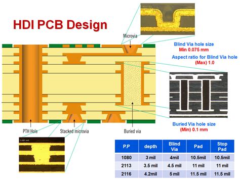
Blind and Buried Vias
In addition to micro vias, HDI PCBs often incorporate blind and buried vias. Blind vias connect an outer layer to an inner layer, while buried vias connect two or more inner layers without reaching the outer layers. These types of vias further enhance the routing flexibility and help in achieving a compact and efficient PCB layout.
Sequential Lamination and Build-up Process
HDI PCBs are manufactured using a sequential lamination and build-up process. This involves building the PCB layer by layer, with each layer being laminated and drilled separately. The build-up process allows for the creation of fine pitch traces and the precise placement of micro vias, ensuring the highest level of interconnect density and reliability.

Designing for HDI PCB Success
Choosing the Right Layer Stack-up
Selecting the appropriate layer stack-up is crucial for HDI PCB success. The stack-up determines the number of layers, their arrangement, and the types of vias used. A well-designed stack-up takes into account signal integrity, power distribution, and manufacturability. It is essential to work closely with your PCB fabricator to determine the optimal stack-up for your specific HDI design.
Component Selection and Placement
When designing an HDI PCB, component selection and placement play a vital role. Choose components with small footprints and fine pitch leads to maximize space utilization. Consider using chip-scale packages (CSPs) and ball grid arrays (BGAs) that are compatible with HDI design rules. Carefully plan the component placement to minimize signal path lengths and ensure proper routing.
Signal Integrity Analysis and Simulation
To ensure the optimal performance of your HDI PCB, it is essential to conduct thorough signal integrity analysis and simulation. Use electronic design automation (EDA) tools to model and simulate the behavior of signals in your HDI design. Analyze factors such as impedance matching, crosstalk, and signal reflections to identify and mitigate potential issues early in the design process.
DFM and Collaboration with PCB Fabricators
Designing for manufacturability (DFM) is critical in HDI PCB development. Engage with your PCB fabricator early in the design process to understand their capabilities, design rules, and recommended best practices. Close collaboration with the fabricator helps in identifying and resolving any manufacturability issues, ensuring a smooth transition from design to production.

HDI PCB Manufacturing Considerations
Material Selection
The choice of materials for HDI PCBs is crucial for achieving reliable and high-performance results. High-quality, low-loss dielectric materials such as polyimide and liquid crystal polymer (LCP) are commonly used in HDI designs. These materials offer excellent electrical properties, dimensional stability, and thermal resistance, making them suitable for demanding applications.
Surface Finish Options
The surface finish of an HDI PCB plays a significant role in its functionality and reliability. Common surface finish options for HDI PCBs include immersion gold (ENIG), electroless nickel/electroless palladium/immersion gold (ENEPIG), and organic solderability preservative (OSP). Each surface finish has its own advantages and considerations, such as cost, shelf life, and compatibility with different assembly processes.
Controlled Impedance and Trace Width Management
Achieving controlled impedance is essential for maintaining signal integrity in HDI PCBs. Careful management of trace widths, spacing, and dielectric thickness is necessary to ensure consistent impedance throughout the board. Work with your PCB fabricator to establish the appropriate trace width and spacing guidelines for your specific HDI design.
Testing and Quality Assurance
Electrical Testing
Thorough electrical testing is crucial to ensure the functionality and reliability of HDI PCBs. Perform continuity tests, insulation resistance tests, and high-potential (hipot) tests to verify the integrity of the connections and the absence of short circuits or leakage paths. Automated test equipment (ATE) can be used to efficiently test complex HDI designs.
Visual Inspection and Microsectioning
Visual inspection is an essential step in the quality assurance process for HDI PCBs. Use microscopes and high-resolution cameras to examine the board for any defects, such as misaligned vias, insufficient solder coverage, or damaged traces. Microsectioning, which involves cross-sectioning the PCB and analyzing the internal structure, can provide valuable insights into the quality of the vias, plating, and lamination.
Reliability Testing
To ensure the long-term reliability of HDI PCBs, it is important to conduct appropriate reliability tests. These tests may include thermal cycling, moisture resistance, and mechanical stress tests, depending on the intended application and operating environment. By subjecting the HDI PCB to these tests, potential weaknesses or failure modes can be identified and addressed before the product reaches the market.
Real-World Applications of HDI PCB
Consumer Electronics
HDI PCBs have become indispensable in the consumer electronics industry. Smartphones, tablets, and wearable devices heavily rely on HDI technology to achieve their compact sizes and advanced features. HDI PCBs enable the integration of high-performance processors, memory modules, and wireless connectivity solutions in these devices, while maintaining a slim and lightweight form factor.
Medical Devices
The medical device industry has greatly benefited from the adoption of HDI PCBs. Miniaturized medical implants, such as pacemakers and neurostimulators, utilize HDI designs to achieve reliable and long-lasting performance within the human body. HDI PCBs also enable the development of advanced diagnostic equipment, surgical instruments, and wearable health monitoring devices, improving patient care and outcomes.
Automotive Electronics
As vehicles become increasingly connected and autonomous, HDI PCBs play a crucial role in enabling advanced driver assistance systems (ADAS), infotainment systems, and vehicle-to-everything (V2X) communication. HDI designs allow for the integration of multiple sensors, processors, and communication modules in a compact and reliable package, enhancing vehicle safety, efficiency, and user experience.
Frequently Asked Questions (FAQ)
-
What is the difference between HDI PCBs and traditional PCBs?
HDI PCBs have higher wiring density, finer pitch components, and micro vias compared to traditional PCBs. They offer advantages such as miniaturization, improved signal integrity, and simplified assembly. -
What are the key technologies used in HDI PCB design?
The key technologies in HDI PCB design include micro vias, via-in-pad, blind and buried vias, and sequential lamination and build-up processes. These technologies enable higher routing density and more complex, multi-layer designs. -
How can I ensure the success of my HDI PCB design?
To ensure the success of your HDI PCB design, choose the right layer stack-up, select appropriate components and placement, conduct signal integrity analysis and simulation, and collaborate closely with your PCB fabricator for design for manufacturability (DFM). -
What materials are commonly used in HDI PCBs?
High-quality, low-loss dielectric materials such as polyimide and liquid crystal polymer (LCP) are commonly used in HDI PCBs. These materials offer excellent electrical properties, dimensional stability, and thermal resistance. -
What testing and quality assurance methods are used for HDI PCBs?
Electrical testing, visual inspection, microsectioning, and reliability testing are important methods used for testing and quality assurance of HDI PCBs. These methods help ensure the functionality, reliability, and long-term performance of the HDI PCB.
Conclusion
HDI PCBs have revolutionized the electronics industry, enabling the development of smaller, faster, and more complex devices. By understanding the key aspects of HDI PCB design, manufacturing, and testing, you can achieve a perfect HDI solution for your specific application. From choosing the right layer stack-up and components to collaborating with PCB fabricators and conducting thorough testing, each step plays a vital role in the success of your HDI PCB.
As technology continues to advance, the demand for HDI PCBs will only continue to grow. By staying up-to-date with the latest trends, techniques, and best practices in HDI PCB development, you can stay ahead of the curve and create innovative, reliable, and high-performance electronic devices that meet the evolving needs of the market.


Leave a Reply