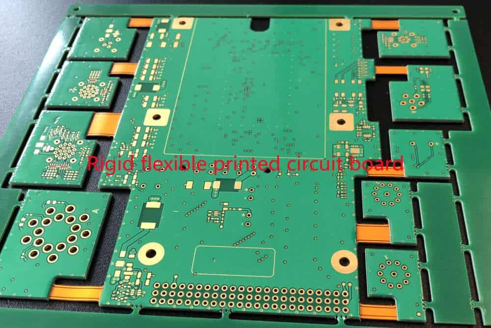
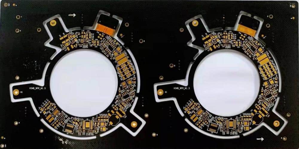
Flexible printed circuit boards (FPCBs) allow electronic connections in applications where rigid boards would be impractical. High-density interconnect (HDI) flex boards take this technology even further, providing advantages like:
- Extremely dense circuitry
- Support for advanced components
- Reduced weight and volume
- Dynamic flexing ability
- Enhanced high-speed performance
With their compact construction and flexibility, HDI flex circuits empower innovations in consumer tech, medical devices, aerospace systems, and more. This article will explore what makes HDI PCBs special and where they enable solutions not possible with other circuit board technologies.
What is HDI Technology for Flexible PCBs?
HDI stands for “high-density interconnect.” It refers to PCBs, both rigid and flexible, that have extremely tight spacing between conductors and small via diameters.
HDI capabilities come from advanced PCB fabrication processes. These include:
- Laser drilling to create microvias under 0.15 mm
- Thin dielectric layers down to 25 μm
- Fine line widths/spaces under 0.075 mm
- Tighter registration accuracy
- Sequential lamination
- Copper-filled microvias
With these techniques, HDI flex boards achieve trace densities over 20,000 nets per square inch. That’s around 4x greater than conventional flexible PCBs.
HDI construction allows placing interconnected components closer together. Pathways between components can be shorter, improving electrical performance. The compact design also minimizes material usage for lighter weight and thinner profiles.
Table comparing HDI and conventional flex board properties:
| Property | HDI Flex Circuits | Conventional Flex Circuits |
|---|---|---|
| Dielectric Thickness | 25-50 μm | 50-100 μm |
| Line/Space | ≤50/50 μm | ≥100/100 μm |
| Microvia Diameter | ≤0.15 mm | ≥0.2 mm |
| Trace Density | >20,000 nets/in2 | ~5,000 nets/in2 |
| Layer Count | 6-8+ | 4-6 |
With minuscule traces, spaces, and vias, HDI enables far greater circuit complexity than normal PCBs. This empowers sophisticated flex board applications.
Key Benefits of Using HDI Flexible PCBs
Why choose HDI instead of standard flex PCBs? Here are some of the main advantages:
Extremely Compact and Lightweight
The small features and thin dielectric layers of HDI technology allow substantial space and weight savings versus conventional flex boards. This enables sleeker, more portable end products.
HDI flex circuits can be over 50% thinner than standard flex PCBs with similar functionality. And the high trace densities require less total board area.
Support for Fine-Pitch Components
Shrinking electronic components call for PCBs with correspondingly fine lines and spaces between circuit paths. HDI flex boards support leading-edge packaging technologies:
- 0201 and 01005 passives
- BGAs with ≤ 0.35 mm pitch
- Flip chip with ≤ 0.3 mm pitch
- MicroBGAs with ≤ 0.25 mm pitch
- Other ultra-fine pitch ICs and connectors
This allows HDI flex circuits to integrate advanced semiconductors for superior product performance.
Multi-Gb/s Data Speeds
HDI construction enhances electrical performance to achieve multi-gigabit data transmission speeds. Shorter distances between components combined with thin dielectric layers provide:
- Lower capacitance for quicker switching
- Tight impedance control for signal integrity
- Reduced cross-talk between traces
The excellent high-speed characteristics suit HDI flex PCBs for rapid data transfer applications.
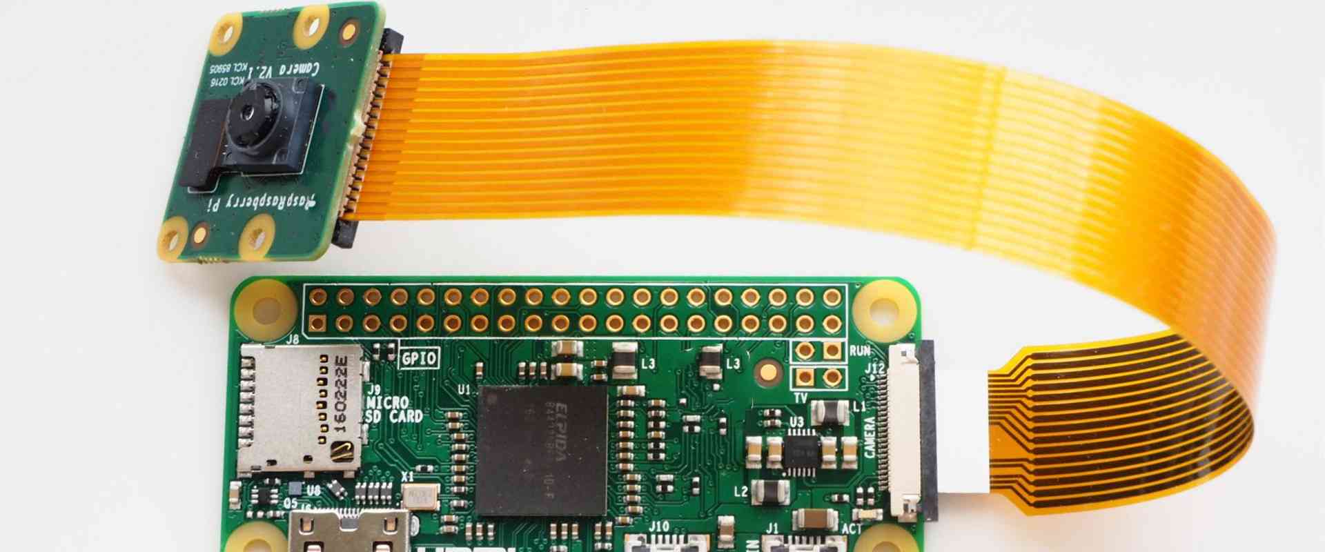
Dynamic Flexing and Bending
Flex-to-install PCBs experience repeated flexing without damage. HDI technology preserves this dynamically flexible nature in high-density circuits.
Through expert layout and advanced materials like polyimide, HDI flex boards can endure millions of flex cycles. This makes them ideal for products with moving or adjustable components.
Reliability
HDI manufacturing processes allow very precise trace characteristics and registration between layers. Plating microvias improves connection reliability versus conventional drilled vias.
Altogether, HDI flex circuits deliver excellent operational reliability under challenging dynamic conditions.
Design Freedom
HDI fabrication enables creative, complex circuit architectures not feasible with other flexible PCBs. With up to 8+ ultra-thin layers interconnected by microvias, these boards provide abundant routing channels.
Circuit designers can optimize layouts to perfectly fit product requirements. And HDI allows high-density connections in flexible sections.
HDI Flex Applications Across Industries
With their advantages, HDI flex circuits find diverse applications in consumer, medical, industrial, aerospace, and other products.
Some examples include:
Consumer Electronics
- Smartphones – Interconnect ultra-thin components
- Tablets/laptops – High-speed low-voltage differential signaling (LVDS) video displays
- Wearables – Lightweight dynamically flexing connections
- Digital cameras – Dense sensor and memory modules with fast data rates
Automotive Industry
- Engine control units – Reliable interconnects in high-heat environments
- Hybrid/electric systems – Complex power and signal distribution
- Advanced driver assistance systems – Tight integration of radar/Lidar sensor arrays
Medical Technology
- Implantable devices – Compact, biocompatible circuits
- Hearing aids – Micro components and flexing reliability
- Endoscopes/catheters – HDI traces through tight tubing bends
Aerospace/Defense
- UAVs – Lightweight HDI boards replace wire harnesses
- Satellites – Rigid-flex links between panels that move after deployment
- Missiles – Circuits enduring launch stresses and wide temperature swings
This list highlights the diversity of HDI flex PCB applications. Any product needing compact, high-speed circuitry with dynamic flexing can benefit from HDI technology.
HDI Flex Board Design Considerations
Developing an optimized HDI flex board requires collaboration between designers and manufacturers. Here are some key design aspects:
Layer Stackup
Selecting dielectric films and copper weights for each layer tailors the stackup to electrical needs and flexing requirements. Important factors are impedance, high-speed performance, and flexibility.
Trace Routing
To benefit from HDI capabilities, layouts must take advantage of the fine features. Critical nets should route on inner layers to shield from noise. And designers should mind trace length matching for differential pairs.
Component Placement
Strategic component placement simplifies routing high-density circuitry. Positioning components with tight relationships near each other improves performance.
Flex Areas
Dynamic bending areas on the board require special attention to avoid damaging traces. Strategies include reinforcing with stiffeners or orienting circuitry properly.
Test Points
Including test points facilitates verifying board function but should minimize effects on flexible regions. Careful positioning maintains their accessibility.
With HDI construction, even small layout choices significantly impact performance. Experienced flex PCB designers are essential to success.
Conclusion
HDI flexible PCBs leverage cutting-edge fabrication techniques to achieve sizes and capabilities beyond conventional flex boards. With high trace densities, micro features, and thin circuit layers, HDI technology enables flexible electronics innovations across many industries. It allows products with compact profiles, dynamic bending requirements, advanced components, and high-speed signals. To fully utilize HDI benefits, designs must employ layout strategies tailored to these unique boards. When engineered effectively, HDI flex circuits deliver superior reliability and functionality.
FQA
What are the key benefits of HDI flex PCBs?
The main benefits of HDI flex PCBs are:
- Extremely compact and lightweight construction
- Support for advanced fine-pitch components
- Multi-gigabit data transmission speeds
- Dynamic flexing and bending reliability
- Precise fabrication for performance and reliability
- Abundant routing channels and design freedom
How are HDI flex boards fabricated?
HDI flex PCBs use special fabrication techniques like laser drilling microvias under 0.15 mm, thin dielectric layers down to 25 microns, fine line widths below 0.075 mm, copper-filled microvias, and sequential lamination. These processes enable trace densities over 20,000 nets per square inch.
What are some applications of HDI flex circuits?
HDI flex PCBs find use in many products like smartphones, wearables, advanced driver assistance systems in cars, satellite panels, and medical implants. Their advantages suit compact consumer electronics, high-speed automotive systems, dynamically flexing aerospace applications, and more.
What design factors should be considered for HDI flex boards?
Critical HDI flex design factors include layer stackup construction, high-density trace routing, strategic component placement, accommodating dynamic flex areas, and including accessible test points. Collaboration between designers and manufacturers ensures optimizing the layout.
How do HDI flexible PCBs differ from conventional flex circuits?
HDI flex boards use thinner dielectric films (25-50 μm vs. 50-100 μm), finer lines/spaces (≤50/50 μm vs. ≥100/100 μm), smaller microvias (≤0.15 mm vs. ≥0.2 mm), and higher trace densities (>20,000 vs. ~5,000 nets/in2). This allows greater circuit complexity in a compact, lightweight format.


Leave a Reply