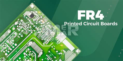
What is FR4 PCB?
FR4 PCB stands for Flame Retardant 4 Printed Circuit Board. It is a type of PCB material that is widely used in the electronics industry due to its excellent mechanical, electrical, and thermal properties. FR4 is a composite material made of woven fiberglass cloth with an epoxy resin binder that is flame resistant.
Composition of FR4 PCB
The composition of FR4 PCB consists of several layers:
| Layer | Material |
|---|---|
| Core | Fiberglass cloth impregnated with epoxy resin |
| Copper foil | Thin layer of copper laminated to the core |
| Solder Mask | Protective layer applied over the copper traces |
| Silkscreen | Layer used for text and symbols |
The fiberglass cloth provides mechanical strength and dimensional stability to the PCB, while the epoxy resin provides insulation and flame resistance. The copper foil is used to create the conductive traces on the PCB, and the solder mask and silkscreen layers provide protection and identification for the traces.
Manufacturing Process of FR4 PCB
The manufacturing process of FR4 PCB involves several steps:
1. Design and Preparation
The first step in the manufacturing process is to design the PCB using CAD software. The design includes the layout of the components, the routing of the traces, and the placement of the holes and vias. Once the design is complete, the data is sent to the PCB manufacturer for preparation.
2. Printing the Circuit Pattern
The next step is to print the circuit pattern onto the copper foil using a photoresist process. The copper foil is coated with a light-sensitive film, and the circuit pattern is transferred onto the film using a high-resolution printer. The film is then exposed to UV light, which hardens the exposed areas of the film.
3. Etching the Copper
After the circuit pattern is printed, the PCB is placed in an etching solution that removes the unwanted copper from the board, leaving only the desired circuit pattern. The etching process is carefully controlled to ensure that the correct amount of copper is removed without damaging the circuit pattern.
4. Lamination
Once the etching process is complete, the PCB Layers are laminated together using heat and pressure. The layers are stacked together and placed in a press, where they are heated and compressed to form a solid board.
5. Drilling
After lamination, the PCB is drilled to create the holes for the components and vias. The drilling process is done using high-speed drill bits that are precisely positioned using CNC machines.
6. Plating
The next step is to plate the holes and vias with copper to create electrical connections between the layers. The PCB is placed in a plating bath, where a thin layer of copper is deposited onto the walls of the holes and vias.
7. Solder Mask and Silkscreen
After plating, a solder mask layer is applied to the PCB to protect the copper traces from oxidation and to prevent Solder Bridges from forming during the soldering process. The solder mask is typically green in color, but other colors are also available.
Finally, a silkscreen layer is applied to the PCB to add text and symbols for identification and assembly purposes.

Advantages of FR4 PCB
FR4 PCB has several advantages over other types of PCB Materials:
- Excellent mechanical strength and dimensional stability
- High insulation resistance and dielectric strength
- Good thermal stability and flame resistance
- Excellent electrical properties, including low dielectric constant and dissipation factor
- Cost-effective and widely available
These properties make FR4 PCB suitable for a wide range of applications, including:
- Consumer electronics
- Telecommunications equipment
- Industrial control systems
- Medical devices
- Automotive electronics

Disadvantages of FR4 PCB
Despite its many advantages, FR4 PCB also has some disadvantages:
- Limited high-frequency performance due to its relatively high dielectric constant and dissipation factor
- Susceptible to moisture absorption, which can cause delamination and other reliability issues
- Not suitable for high-temperature applications above 130°C
- May contain hazardous substances such as bromine and lead, which can be harmful to the environment and human health

Alternative Materials to FR4 PCB
For applications that require higher performance or more specialized properties than FR4 PCB can provide, there are several alternative materials available:
High-Frequency Materials
For high-frequency applications, such as RF and microwave circuits, materials with lower dielectric constants and dissipation factors are required. Some common high-frequency materials include:
- Rogers RO4000 series
- Isola IS680
- Taconic RF-35
These materials offer excellent high-frequency performance, but they are more expensive than FR4 and may require specialized processing techniques.
High-Temperature Materials
For applications that require operation at high temperatures, such as aerospace and automotive electronics, materials with higher glass transition temperatures (Tg) are required. Some common high-temperature materials include:
- Polyimide (PI)
- Bismaleimide triazine (BT)
- Cyanate ester (CE)
These materials can withstand temperatures up to 250°C or higher, but they are more expensive than FR4 and may require specialized processing techniques.
Environmentally-Friendly Materials
For applications that require environmentally-friendly materials, there are several options available that do not contain hazardous substances such as bromine and lead. Some common environmentally-friendly materials include:
- Halogen-free FR4
- Polyphenylene oxide (PPO)
- Polyethylene terephthalate (PET)
These materials offer similar properties to traditional FR4, but they are more environmentally friendly and may be required for certain applications or markets.
Frequently Asked Questions (FAQ)
- What does FR4 stand for in PCB manufacturing?
-
FR4 stands for Flame Retardant 4, which is a type of material used in the manufacturing of printed circuit boards (PCBs).
-
What is the composition of FR4 PCB?
-
FR4 PCB is composed of a core layer of fiberglass cloth impregnated with epoxy resin, with copper foil laminated on top and bottom surfaces for electrical conductivity. It also includes a solder mask layer for protection and a silkscreen layer for identification.
-
What are the advantages of using FR4 PCB?
-
FR4 PCB has several advantages, including excellent mechanical strength, high insulation resistance, good thermal stability, and excellent electrical properties. It is also cost-effective and widely available.
-
What are some applications of FR4 PCB?
-
FR4 PCB is used in a wide range of applications, including consumer electronics, telecommunications equipment, industrial control systems, medical devices, and automotive electronics.
-
Are there any alternative materials to FR4 PCB?
- Yes, there are several alternative materials available for applications that require higher performance or more specialized properties than FR4 PCB can provide. These include high-frequency materials like Rogers RO4000 series, high-temperature materials like polyimide (PI), and environmentally-friendly materials like halogen-free FR4.


Leave a Reply