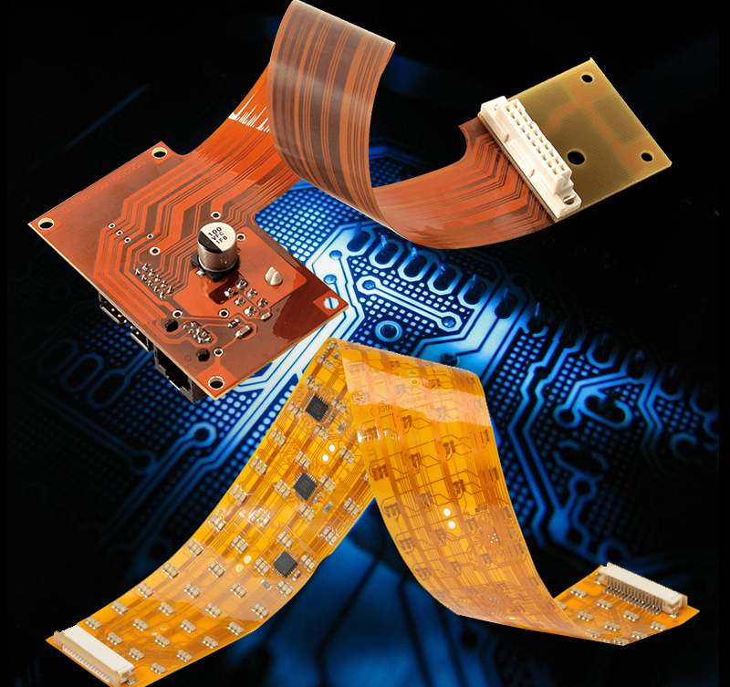
Introduction
Flexible printed circuit boards (PCBs) have become increasingly popular in recent years due to their ability to bend and flex to fit within tight spaces. Choosing the right thickness is critical when designing a flexible PCB, as the thickness impacts the circuit’s durability, flexibility, and electrical performance. This article will provide a comprehensive guide on flexible PCB thickness, including how thickness affects performance, common thicknesses used, and tips for selecting the right thickness for your application.
How Thickness Impacts Flexible PCB Performance
The thickness of the copper and polyimide layers in a flexible PCB directly impacts several aspects of performance:
Durability
Thicker flex circuits are more durable and resistant to mechanical stress. Thin circuits below 0.0005” are quite fragile while thickness above 0.005” are very robust.
Flexibility
Thinner flex circuits can bend into tighter radii than thicker ones. Minimum bend radius typically increases linearly with thickness.
Electrical Performance
Thicker copper provides lower electrical resistance while thinner copper allows for finer traces and spacing. Ideal impedance matching also depends on copper thickness.
Weight and Space
Thinner flex circuits minimize weight and maximize the use of space in tight, compact devices.
Finding the ideal balance of these factors based on your particular application requirements is key to selecting the right flexible PCB thickness.
Common Flexible PCB Thicknesses
Flexible PCBs are available in a wide range of thicknesses, from as thin as 0.0005” up to 0.010” or more. Here are some of the most common thicknesses used:
| Thickness | Type | Description |
|---|---|---|
| 0.0005” | Ultra-thin | Extremely fragile but highly flexible |
| 0.001” | Thin | Lightweight, cost-effective, short flex life |
| 0.002” | Standard | Balances flexibility, durability, and cost |
| 0.003” | Thick | Robust and rigid but less flexible |
| 0.005”+ | Extra thick | Maximum durability for high stress |
0.001”, 0.002”, and 0.003” are considered the most popular thicknesses for typical flexible PCB applications. 0.0005” is often used when extreme flexibility and space savings are needed, while 0.005”+ is reserved for very demanding environments.
Tips for Selecting the Right Thickness
Choosing the ideal flexible PCB thickness depends on carefully evaluating your specific design needs. Here are some useful tips:
- Consider minimum bend radius – Thinner PCBs can fold into much tighter radii than thicker ones. Know the sharpest bends needed.
- Analyze required durability – Will the flex circuit experience significant vibration or repeated motion? Thicker may be better.
- Review circuit complexity – Thinner can accommodate finer traces and spaces for complex circuitry.
- Assess space requirements – Thinner flex circuits maximize limited space in compact devices.
- Know expected life cycles – Thinner flexes often have shorter life cycles. Thicker may last longer.
- Review electrical needs – Thicker copper provides lower resistance. Determine ideal trace sizes.
- Consider cost – Thinner flexes typically have lower material costs but may not last as long.
- Select an experienced manufacturer – Their guidance can help identify the best thickness for your design.
Prototyping multiple thicknesses is recommended to empirically determine the ideal flex, form, and function.
Flexible PCB Thickness Guidelines by Application
The table below provides general thickness guidelines for some common flexible PCB applications:
| Application | Recommended Thickness Range |
|---|---|
| Wearable devices | 0.001” – 0.002” |
| Tight cabling, coils | 0.0005” – 0.002” |
| Consumer electronics | 0.002” – 0.003” |
| Automotive, industrial | 0.002” – 0.005”+ |
| High flex connectors | 0.001” – 0.003” |
| Military, aerospace | 0.002” – 0.005”+ |
| Medical devices | 0.001” – 0.003” |
Of course, these are rough recommendations and the ideal thickness depends on each design’s specific requirements. Work closely with your flex PCB manufacturer to dial in the perfect thickness.
Design Rules and Limitations by Thickness
As flexible PCB thickness decreases, certain design rules and limitations begin to apply:
- Trace/space reduces – Thinner copper requires finer lines and spaces
- Bend radius increases – Tighter folds require thinner material
- More fragile – Risk of tears or cracks goes up
- Lower current capacity – Thin tracks can’t handle high amperage
- Impedance control harder – Varying dielectric thickness impacts impedance
- Lower stiffness – Thin flexes require structural support
- Shorter life cycle – High-flex designs wear faster
Carefully following all design guidelines for the selected thickness helps mitigate these limitations and results in a robust, high-performing flex circuit design.
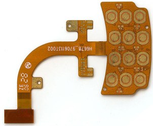
Flex Stackups: Copper/Polyimide Layer Options
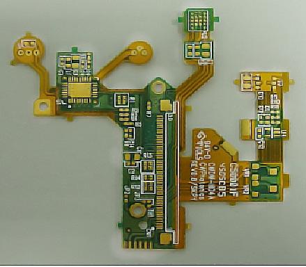
In addition to the overall thickness, flexible PCB constructions can use different copper and polyimide layer combinations known as flex stackups. Common options include:
- Single-sided – One copper layer on one side of the polyimide. Low cost but less flexible.
- Double-sided – Copper on both sides. Allows more complex circuitry.
- Multilayer – Two or more copper layers separated by polyimide. Enables high-density flex circuits but is more expensive.
- Rigid-flex – Combines stiff PCB sections with flexible joints. Multilayer flex stacked with rigid boards.
The stackup design impacts the overall thickness as well as the flex circuit’s durability and circuit density.
Prototyping: Accelerating Flex Design Iteration
Prototyping multiple flexible PCB thickness variants is highly recommended during the design process to validate the ideal thickness. Cost-effective prototyping options include:
- Low-volume batches – Start with small batches of 5-10 boards at varying thicknesses. Test form, fit, and function.
- On-demand manufacturing – Use agile vendors to ship fast iterations of different thicknesses.
- Panel sharing – Share panel space across customers to lower cost.
Leveraging prototyping minimizes risk by optimizing thickness before higher volume production.
Conclusion
Choosing the right thickness is one of the most critical design decisions when developing flexible PCBs. Thinner circuits provide extreme bendability but sacrifice durability, while thicker flexes are robust but less flexible. Selecting the ideal balance requires carefully analyzing the flex circuit’s mechanical, electrical, and functional requirements. Areas like minimum bend radius, expected life cycle, circuit complexity, and cost targets all factor into the thickness equation. Following design rules and leveraging prototyping reduces risk and results in an optimized flex circuit thickness tailored exactly for the application.
Frequently Asked Questions
Q: What is the minimum thickness for flexible PCBs?
A: The minimum thickness for flexible PCBs is typically around 0.0005″ (0.5 mil). This ultra-thin dimension provides maximum flexibility to bend into tight radii but the circuits are extremely fragile at this thickness. Most flex PCBs range from 0.001″ to 0.005″ for the best balance of flexibility, durability, and performance.
Q: How does flexible PCB thickness impact bend radius?
A: Thinner flex circuits can bend into much tighter radii than thicker ones. As a general guideline, minimum bend radius increases linearly with thickness. For example, 0.001″ material can bend to a 0.010″ radius, while 0.003″ would require at least a 0.030″ radius. Tighter bend radii require thinner flexible PCB material.
Q: When would a thicker vs. thinner flex PCB be used?
A: Thinner flex PCBs (0.001-0.002″) maximize flexibility and space, making them ideal for compact wearables and consumer electronics. Thicker flexes (0.003-0.005+”) provide robustness and durability for high vibration, repeated flexing, and long product life cycles like in automotive or industrial uses. The right thickness depends on balancing flexibility, longevity, and performance.
Q: How does flexible PCB thickness impact manufacturability?
A: Thinner flex circuits allow for finer trace and space designs but require tighter process controls. Thicker flex PCBs are easier to manufacture but limit circuit density. In general, once below 0.002″, specialized tools and handling are needed to manufacture thin flex reliably. Work closely with your flex PCB vendor to ensure their capabilities match your design needs.
Q: Does flex PCB thickness affect signal transmission?
A: Yes, flexible PCB thickness impacts a few aspects of electrical performance. Thinner copper increases resistivity while thicker copper improves conductivity and reduces losses. Thinner dielectrics also make it more difficult to tightly control impedance. However, thinner traces enable higher densities. It’s a balancing act to optimize thickness for the design’s speed, power, and signal integrity requirements.


Leave a Reply