Introduction to Flexible PCBs
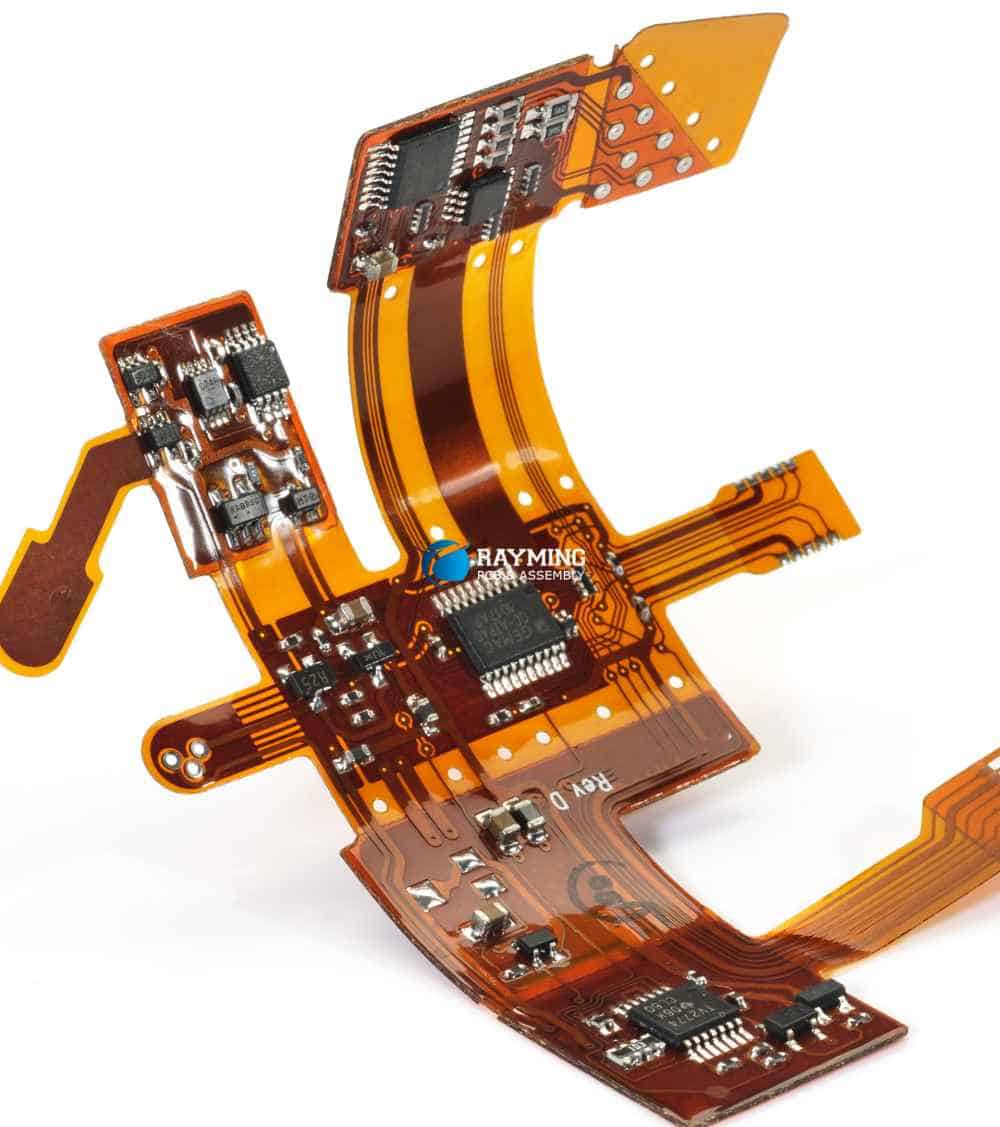
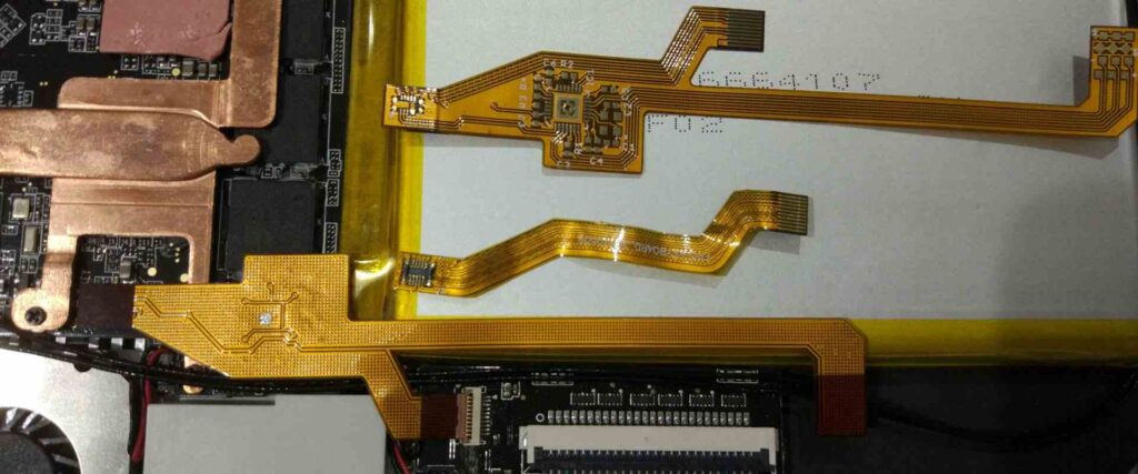
A flexible printed circuit board (PCB) is a type of PCB made of flexible insulating material with conductive traces printed or bonded on top. Unlike rigid PCBs which are made of stiff insulating materials like FR4, flexible PCBs can bend and twist to fit into tight or movable spaces in electronic devices.
Some key advantages of flexible PCBs include:
- Flexibility – Can bend and flex repeatedly without damage
- Lightweight – Much thinner and lighter than rigid boards
- Durability – Highly resistant to vibration and shock
- Customizable – Can be fabricated in many shapes and sizes
- Signal integrity – Excellent electrical performance with controlled impedance
Flexible PCBs are ideal for applications where flexibility, weight, space savings, or vibration resistance are important factors. They are commonly used in consumer electronics, medical devices, industrial equipment, aerospace systems, and more.
Why Prototype Flexible PCBs?
Prototyping is an important part of the flexible PCB design process. Here are some key reasons to prototype flexible PCBs before full production:
Verify Design and Functionality
Prototyping allows you to test your flexible PCB design and confirm it works as intended before manufacturing a full production run. You can check for errors in the layout, test component fit and placement, and validate the overall functionality. Prototypes give you an early opportunity to correct any issues.
Evaluate Manufacturing Process
Creating prototype boards helps qualify your manufacturing and assembly processes before ramping up to full-scale production. You can assess the chosen flexible PCB fabricator and assembly contractor using prototype boards.
Make Design Iterations
Prototypes make it faster and easier to test design changes compared to re-spinning an entire production run. You can tweak the layout, swap components, or make updates to fix issues found during prototyping.
Reduce Development Risks
Finding design flaws or manufacturing issues during prototyping when volumes are low reduces risk, time and cost. It avoids problems cropping up after launching a finished product. Overall, prototyping leads to higher quality finished boards.
In summary, flexible PCB prototyping is invaluable for confirming the design, evaluating manufacturability, making iterative improvements, and ultimately reducing development risk.
Flexible PCB Prototype Design Considerations
Here are some important design factors to consider when prototyping flexible PCBs:
Layer Stackup
Determine the necessary number of copper layers and dielectric materials for your design requirements. More layers provide higher routing density but increase costs.
Circuit Density
Optimizing component placement and routing for efficient use of space. Balance density needs with manufacturability.
Bend Radius
Account for required bend radius of flexible circuits and distances to neutral axis. Avoid over-stressing boards during flexing.
Panel Utilization
Maximize board space on panel to minimize prototyping costs. But allow room for test points, fiducials, and tooling holes.
Board Outline
Define board shape and locations of tooling holes, fiducials, and breakaway tabs for board separation.
Test Points
Add test points for probing signals and checking voltages during prototype evaluation. But minimize excess pads.
Stiffeners
Determine if stiffeners are required to prevent flexing in certain areas for component protection.
Coverlay Openings
Identify openings in solder mask for soldering components, display windows, connectors etc.
These guidelines help optimize the prototype design for manufacturability and performance.
Flexible PCB Prototype Manufacturing Process
Here is a typical workflow for manufacturing prototype flexible PCBs:
1. Design Creation
A PCB layout tool like Altium or Cadence is used to design the flexible board and output Gerber files.
2. Design Verification
The PCB designer reviews the layout and Gerber files to verify all specifications are met. Design rule checks are run.
3. Prototype Order
A purchase order is sent to a flexible PCB manufacturer and Gerber files are uploaded for prototyping.
4. CAM Processing
The manufacturer processes the Gerber files through CAM software to generate tooling and fabrication data.
5. Panel Preparation
One or more PCB designs are arranged on a panel to optimize board space. Tooling holes and fiducials are added.
6. Lamination
Thin insulating dielectric layers and copper foils are stacked then laminated under heat and pressure.
7. Imaging
Photoresist is applied and imaged to transfer the circuit pattern from artwork films to the copper layers.
8. Etching
Chemicals dissolve away unwanted copper to leave only the desired conductive traces.
9. Strip and Clean
The photoresist is stripped away and surfaces are cleaned in preparation for coverlay application.
10. Coverlay
A protective solder mask layer is laminated over the top and bottom copper layers.
11. Singulation
Individual PCBs are separated by cutting through breakaway tabs around the board outlines.
12. Testing and Shipment
Each board undergoes electrical testing before shipment to the customer.
This typical flexible PCB prototype workflow ensures an efficient manufacturing process and high-quality boards. Minor process adjustments may be required for different materials used.
Assembling Flexible PCB Prototypes
Once the bare flexible PCB prototypes are received from fabrication, they are ready for component assembly. Here is a general FPC assembly process flow:
1. Solder Paste Printing
Solder paste is screen printed or dispensed on pads for surface mount device attachment.
2. SMD Placement
Pick-and-place machines populate the SMDs onto the solder paste deposits on the boards.
3. Reflow Soldering
The boards pass through a reflow oven to heat the solder paste and attach the components.
4. Conformal Coating
A protective coating may be selectively applied over the assemblies.
5. Aqueous Cleaning
Any post-assembly fluxes are washed off the boards using cleaners.
6. Programming
For boards with programmable devices like microcontrollers, firmware is loaded.
7. Testing
Each populated PCB undergoes electrical testing and inspection to confirm functionality.
8. Packaging and Shipment
The finished prototype assemblies are packed and shipped to the customer.
Depending on complexity, some flexible PCB prototypes may require additional assembly steps like adhesive attachment, press-fit connectors, mechanical assembly, etc. But this general assembly sequence applies to most standard FPC prototypes.
Tips for Successful Flexible PCB Prototypes
Here are some helpful tips to ensure your flexible PCB prototypes meet requirements:
- Leave room in the layout for design tweaks between prototype iterations.
- Build in testability by including testpoints and ground vias for probing.
- Clearly specify prototyping needs upfront to the PCB manufacturer.
- Perform design reviews before prototyping to catch issues early.
- Get assembly quotes to budget for parts costs before prototyping.
- Work closely with your PCB supplier to understand their prototyping capabilities.
- Build a complete prototype with all components first, then simplify if possible.
- Evaluate the first prototypes before ordering additional boards.
- Test prototypes thoroughly against all specifications and requirements.
- Make notes for improvements to address in the next design revision.
Following these guidelines will help you get the most value out of flexible PCB prototyping and avoid pitfalls.
FQA
What are the typical layers used in flexible PCB prototypes?
Typical flexible PCB prototypes have 1-4 layers. Single layer flex circuits are inexpensive and offer basic flexibility. 2-4 layer prototypes provide more complex routing while maintaining decent flexibility. Typical dielectric materials are polyimide and polyester films.
What are some best practices for designing flex PCB prototypes?
Some best practices include: optimize routing to avoid 90 degree traces, design teardrop pads for better soldering, minimize unsupported spans of conductors, keep rigid sections short, use hatched copper fills for better flexibility, and add strain relief features.
What file formats do PCB manufacturers need for prototypes?
Manufacturers need Gerber files (RS-274X) for each layer, drill files, netlist, assembly drawings, centroid data, and documentation like readme files and IPC netlist class definitions.
How long does it take to get flexible PCB prototypes?
With expedited services, you can typically get prototypes in 5-7 days. Standard turn times are around 10-15 days. For complex boards with buried vias, expect 15-20 days.
How many prototype iterations are typically needed?
2-3 iterations is typical to fix any bugs in the design. The first prototype validates the basic design. The second prototype refines it. Additional prototypes incorporate any last optimizations.


Leave a Reply