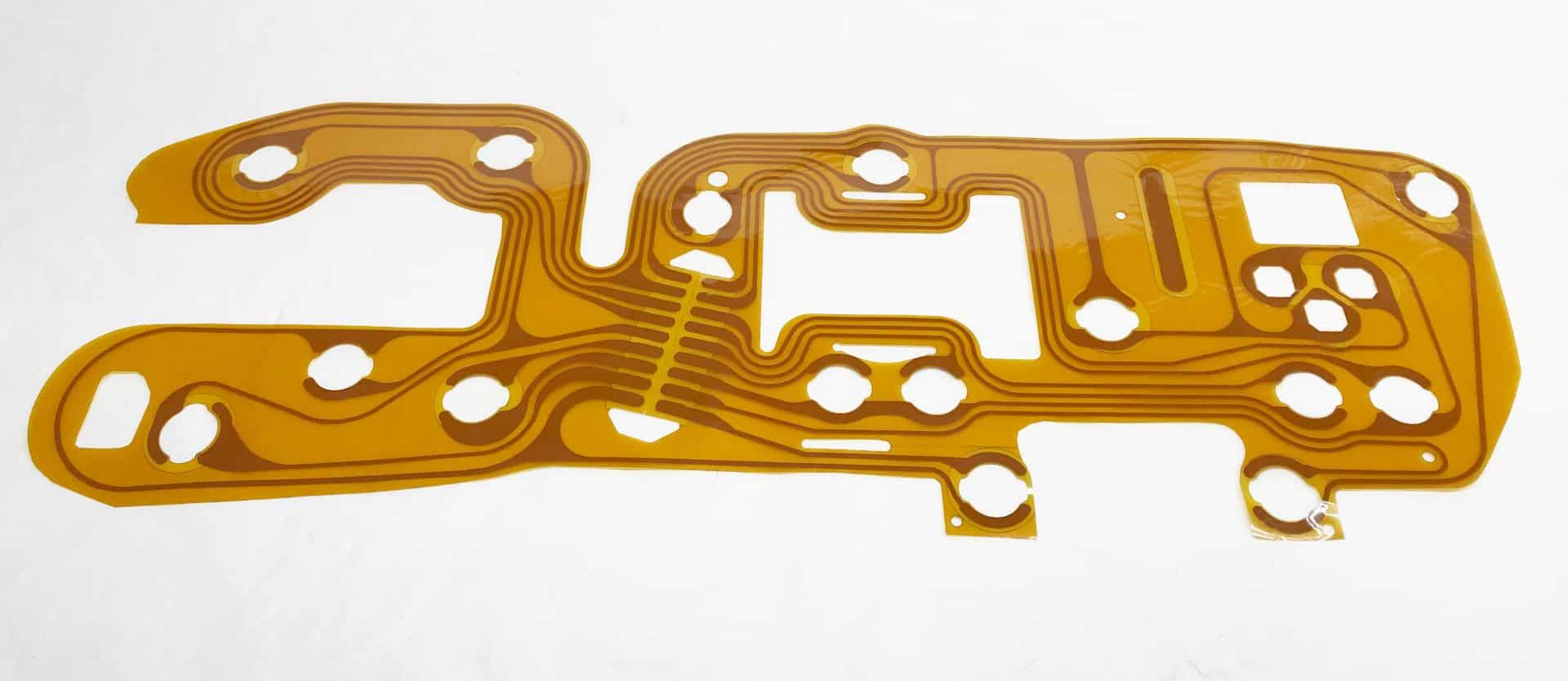
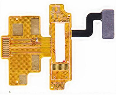
Flexible printed circuit boards (flex PCBs) offer unique advantages over traditional rigid PCBs, including flexibility, dynamic bendability, and space/weight savings. However, designing flex PCBs requires special considerations to ensure reliability and performance. This guide provides key flex PCB design guidelines and tips for optimizing your flexible circuits.
Choose the Right Flexible Substrate Material
Choosing the appropriate flexible substrate is one of the most critical aspects of flex PCB design. The substrate material determines the circuit’s flexural endurance, electrical performance, and cost. Here are some key considerations when selecting a flex substrate:
Dielectric Material
- Polyimide films like Kapton provide excellent thermal stability and flex life but are more expensive.
- Polyester films are affordable but have lower maximum operating temperatures.
- PEN and PET films offer good value and performance balance.
- Composite substrates reinforce polymer films with glass fiber for rigidity in parts of the circuit.
Copper Foil Type
- Rolled annealed copper is highly ductile for dynamic flexing.
- Electrolytic tough pitch copper foil is less expensive but more prone to cracking.
- Very thin foils (down to 1-2μm) maximize flexibility.
Film Thickness
- Typical flex circuit thicknesses range from 25-100μm.
- Minimum thickness depends on required voltage isolation.
- Thinner substrates maximize bend radius.
Optimize Flexible PCB Layer Stackup
Carefully planned layer stackup is key to avoiding failures like delamination and cracking during flexing. Follow these stackup design guidelines:
Symmetrical Construction
- Use symmetrical stackups (equal layer counts on both sides of center plane) to prevent curling.
- Unbalanced constructions require stiffeners or thicker cover layers.
Adhesive Selection
- Acrylic and urethane adhesive provide the best bond strength for dynamic flexing.
- Epoxies have higher glass transition temperatures but are more brittle.
Coverlayer Thickness
- Use thicker coverlayers over conductors subjected to repeated flexing stresses.
- 25-50μm covers are typical; up to 125μm for high flex areas.
Design for Maximum Flexibility
Optimizing flex circuit patterns is vital for reliable dynamic bending and flexing:
Trace Routing
- Route traces in the neutral bending axis whenever possible.
- Avoid traces perpendicular to the bend direction.
Coverlayer Openings
- Avoid openings in coverlayers over conductors in flex areas.
- Openings can be used in rigid areas.
Annular Rings
- Use larger annular rings around plated through holes for enhanced reliability.
- 50-75μm annular rings are typical in rigid sections.
- 100-200μm rings should be used in dynamic flex zones.
Stress Reliefs
- Add teardrop shapes at trace corners in flexing regions to reduce stress concentrations.
- Rounded traces and terminals further improve dynamic flex life.
Design Rigid Areas for Support

While flexible zones provide the dynamic bending of flex circuits, some rigid sections are required for:
Component Mounting
- Use discrete rigid “islands” for attaching IC packages and connectors.
- Avoid components in highly dynamic flexing areas.
Stiffening and Support
- Rigid sections reinforce the circuit and facilitate handling and assembly.
- Don’t over-stiffen the board as it reduces flexibility.
Multilayer/High Density
- Rigid sections enable creation of multilayer and high density flex-rigid boards.
- Flex layers interconnect the rigid sections.
Model and Test the Design
Analysis and testing of flex PCB designs are critical to avoid problems during actual flexing:
CAD Stress Analysis
- Use FEA tools in CAD software to model stresses and identify failures.
- Optimize routing, layer stackup, and bend areas based on results.
Prototyping and Testing
- Test multiple prototypes with increasing bend cycles until failure occurs.
- Inspect closely for cracks and delamination issues.
- Identify improvements from root cause failure analysis.
Preconditioning
- “Break-in” manufactured circuits prior to service through repeated flexing.
- Starts with low stress cycles, increasing over time.
- Removes defects and stabilizes materials.
Partner with an Experienced Flex PCB Manufacturer
While these guidelines will help optimize your flex PCB design, it’s also essential to work with a manufacturer specializing in flexible circuits. Benefits include:
- Expert design review and recommendations
- Material selection assistance
- Prototyping capabilities
- Comprehensive testing services
- Advanced flex PCB fabrication processes
- Effective quality control and inspection
Partnering with an expert flex PCB company reduces risks and ensures you get a well-designed, thoroughly tested flex circuit that meets your requirements.
FQA
What are the main advantages of using flex PCBs vs. rigid PCBs?
Some key advantages of flex PCBs include:
- Dynamic flexing and bending abilities
- Thinner, lighter weight, and more space efficient
- Improved reliability in motion applications
- Can conform to challenging geometries
- Enable creative packaging innovations
- Simpler, lower cost assembly in many cases
What are some typical applications suited for flexible circuits?
Flex PCB’s are well suited for:
- Consumer devices (laptops, mobile phones, wearables)
- Portable medical devices
- Automotive cameras and sensors
- Aerospace and military systems
- Industrial robotics and machine controls
Any application where flexibility, space savings, or dynamic bending is useful can benefit from incorporating flex circuits.
What are some best practices when routing conductors on flex PCBs?
Routing guidelines include:
- Place traces along the neutral bend axis whenever possible.
- Avoid perpendicular traces crossing flex zones.
- Use curved rather than angular trace patterns.
- Add teardrop pads at trace corners in dynamic areas.
- Remove coverlayer dielectric over traces in high flex zones.
How can designers ensure good flex life and avoid cracking/fatigue?
To optimize flex life:
- Use flexible but resilient substrate materials like polyimide.
- Incorporate stress relief features on traces.
- Allow sufficient spacing between conductors.
- Add stiffeners and reinforcements where needed.
- Verify design through FEA stress analysis.
- Perform physical testing via flex cycling.
What are some considerations when integrating rigid and flex sections?
Guidelines for rigid-flex integration:
- Place components only on rigid sections.
- Use symmetric layer stackups to avoid curling.
- Allow sufficient clearance for flex bending at transitions.
- Anchor flex layers thoroughly in rigid sections.
- Include interlayer stiffeners between flex/rigid sections.


Leave a Reply