Introduction
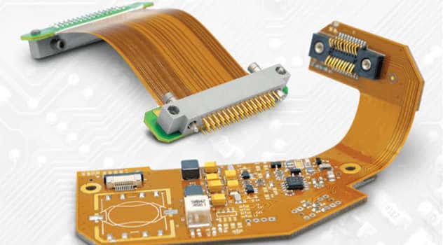
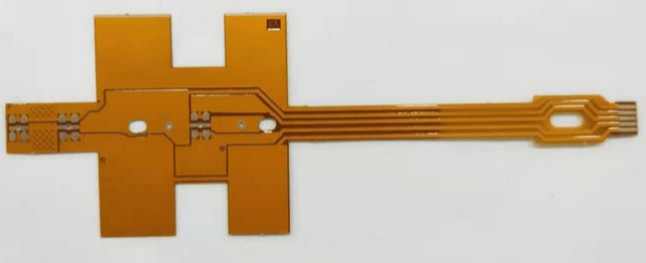
Flexible printed circuit boards (flex PCBs) are a critical component in many modern electronic devices. As devices get smaller and more portable, flex PCBs allow circuitry to bend and flex with the device. A key consideration when designing a flex PCB is the thickness of the copper traces. Selecting the right copper thickness is essential to ensure reliability and performance. This article will examine the factors that determine ideal copper thickness for flex PCBs.
Copper Thickness Basics
The copper traces on a flex PCB carry the electric signals between components. Copper thickness is measured in ounces per square foot (oz/ft2). Typical thicknesses used are 1/4 oz (0.7 mil), 1/2 oz (1.4 mil), 1 oz (2.8 mil), and 2 oz (5.6 mil). Thicker copper has lower resistivity, allowing more current to flow. But thicker copper is less flexible and more prone to cracking. Determining the right thickness requires balancing conductivity vs. flexibility.
Here are some of the tradeoffs between thin and thick copper for flex PCBs:
Thin Copper (1/4 to 1/2 oz)
- More flexible, can bend to tighter radii
- Lower weight
- Lower cost
- Higher resistivity, limiting current
Thick Copper (1 to 2 oz)
- Excellent conductivity and current capacity
- More resilient to flexing fatigue
- Added rigidity, may be undesirable
- Higher weight and cost
- Less flexible, higher bending radius
Hybrid Thickness
- Common to use 1/2 oz for traces, 1 oz for power areas
- Balances flexibility and conductivity
Factors That Determine Optimal Copper Thickness
There are several key factors that influence the ideal copper thickness for a particular flex PCB design. These include:
Circuit Currents and Trace Lengths
Higher currents and longer trace lengths require thicker copper to limit voltage drops. Sensitive signals like clocks may need thicker traces. Power traces over 1 amp usually need at least 1 oz.
Amount of Flexing
Circuits with dynamic flexing during use need thinner copper to endure repeated bending. Static flex circuits can utilize thicker copper.
Bending Radius
The sharpest bend a circuit will encounter determines the minimum bend radius. Thinner copper allows for tighter bend radii.
Layer Count
Adding more copper layers enables the use of thinner copper per layer. It helps limit increases in thickness and rigidity.
Environmental Conditions
Thicker copper is more resistant to damage from abrasion, chemicals, and environmental exposure. Flex circuits in harsh conditions may benefit from thicker copper.
Component Placements
Avoid placing heavy components in areas that bend, as this can concentrate stresses. Strategic component placement reduces cracking risks.
Manufacturing Process
The PCB fabricator’s capabilities for handling thin materials influences the minimum copper thickness. Electroless copper plating allows thinner starting layers.
Recommended Copper Thickness Guidelines
Here are some best practice recommendations for selecting copper thickness on flex PCBs, depending on different design considerations:
Low Current/Static Flex Circuits
- 1/4 to 1/2 oz copper should suffice
- Allows tight bend radii down to 2-3 mm
Dynamic Flexing Applications
- Use 1/2 oz for all traces
- Up to 1 oz for power lines
- Bend radii 4-5 mm minimum
High Current and Large Flex PCBs
- 1 oz copper minimum for all traces
- 2 oz for high current power traces > 3A
- Larger bend radii, 5-10 mm minimum
Extreme Flexing/Roll-Up Circuits
- 1/4 oz traces, 1/2 oz power pads
- Consider adding polyimide stiffeners for strain relief
- Bend radii 10 mm or greater
Multilayer Flex PCBs
- 1/4 to 1/2 oz traces per layer
- Total copper >2 oz for power areas
- Thicker dielectrics to reduce layer count
Improving Flexibility With Annealing
Annealing the copper foil is an important process step to enhance flexibility. Annealing relaxes the crystalline structure of the foil, making it less brittle. This enables thinner copper foils to be used, while maintaining resilience to repeated bending stresses.
The annealing process involves heating the copper foil until it recrystallizes, then cooling it down slowly. This reduces grain size and internal stresses. With proper annealing, 1/4 oz copper can achieve over 10,000 bending cycles.
The PCB fabricator should be consulted to ensure proper annealing will be performed. This is critical for dynamic flexing applications.
Reinforcement Options
For high flex circuits, additional reinforcements can be added to improve robustness:
- Stiffeners: Polyimide films around bend areas help distribute stresses.
- Solder Mask Buildup: Additional layers of solder mask increase thickness.
- Adhesives: Acrylic or epoxy adhesives are applied to static areas.
- Buried Cores: Polyimide or FR4 layers are embedded internally.
Reinforcements provide support to high stress zones. This allows thinner copper to be used while still meeting durability requirements.
Summary
- Thinner copper improves flexibility while thicker copper enhances conductivity.
- Match copper thickness to current levels, trace lengths, and flexing requirements.
- Follow recommended guidelines, using 1/2 to 1 oz for most moderate flex applications.
- Annealing enhances the fatigue resistance of thin copper foils.
- Additional reinforcements can mitigate bending stresses.
- Work with your PCB supplier to validate minimum copper thickness.
Carefully balancing copper thickness and reinforcements allows even the most demanding flex circuit designs to succeed. With the right thickness, flex PCBs can maintain superior reliability while enabling the subtlest bend radii.
Frequently Asked Questions
Q: What is the minimum copper thickness that can be used on a flex PCB?
A: The thinnest flex PCB copper foils are around 1/4 oz (0.7 mil). However, 1/2 oz (1.4 mil) is more commonly used as the minimum thickness for reliability. Electroless copper plating can deposit thinner copper down to 0.1 mil for the starting layer.
Q: How do I know if I should use 1 oz or 2 oz copper thickness?
A: 1 oz should handle the majority of flex PCB applications. Use 2 oz only for high current power lines over 3-5 amps, or in very harsh environments. The added thickness and loss of flexibility of 2 oz copper makes it suitable for selective areas only.
Q: What is the effect of bending radius on copper thickness selection?
A: Tighter bending radii require thinner copper to avoid cracking. As a guideline, 1/2 oz copper allows a 2-3 mm radius, 1 oz copper is 4-5 mm, and 2 oz copper is over 10 mm. The minimum bend radius grows exponentially as copper thickness increases.
Q: Can different copper weights be used on the same flex PCB?
A: Yes, it is common to use different thicknesses on one design. For example, 1/2 oz traces with 1 oz power distribution lines. This allows optimization of flexibility and conductivity in respective areas. Gradually transition between different thicknesses.
Q: How many times can a flex PCB be bent before the copper traces crack?
A: Properly annealed 1/2 oz copper can achieve over 10,000 dynamic bending cycles. Addition of stiffeners and protective layers can further improve flex life. Thinner copper generally endures more cycles before cracking than thicker layers.


Leave a Reply