Introduction
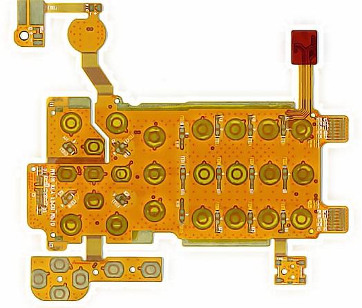
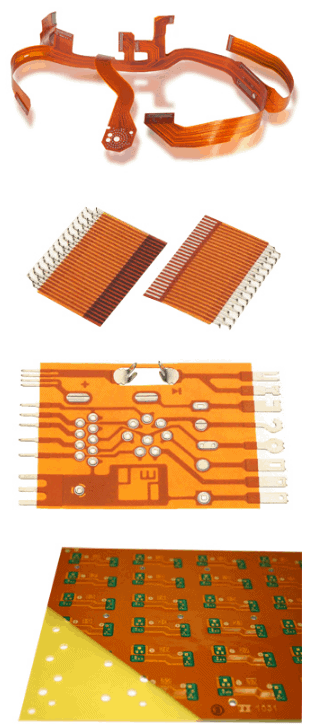
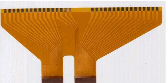
Flex circuits, also known as flexible printed circuits, are thin circuits made from copper traces bonded to flexible substrates like polyimide or polyester. Compared to traditional rigid printed circuit boards, flex circuits can bend and flex to fit unique form factors and move dynamically in electronic devices.
Determining the right thickness for a flex circuit is an important design consideration impacting the circuit’s electrical, mechanical, and thermal performance. This article provides a detailed overview of how flex circuit thickness affects key parameters and provides guidance on selecting the optimal thickness for your application.
How Thickness Impacts Flex Circuit Performance
Flex circuit thickness, typically measured in mils (1/1000 inch), can range from as low as 1 mil to more than 10 mils. While thinner circuits are desirable for flexibility and space savings, the thickness must be adequate to meet circuit requirements. Key factors impacted by thickness include:
Electrical Performance
- Conductor resistance – Thinner circuits have higher resistivity, potentially impacting voltage drop over long trace lengths. For high current applications, thicker copper and substrates may be required.
- Impedance control – Thinner dielectrics reduce spacing between copper layers, making it more challenging to achieve target impedance for high speed signals.
- Insulation resistance – Thinner circuits are more prone to pinholes and dielectric breakdown, reducing insulation resistance.
- Withstand voltage – The voltage that can be continuously applied without dielectric failure decreases for thinner flex circuits.
Mechanical Performance
- Bend radius – Minimum bend radius increases proportionally with thickness. Thicker flexes are less capable of dynamic flexing and fitting small form factors.
- Bond strength – Thicker adhesives and copper help prevent delamination and cracking on dynamic and high stress flex applications.
- Stiffness – Thicker circuits are less flexible and may require scoring or selective thinning in high flex zones.
Manufacturing Considerations
- Handling and processing – Thinner circuits can be prone to damage during assembly and require extra care in handling.
- Registration accuracy – Alignment of thin circuits for sputtered coatings and photolithography can be more challenging.
- Component spacing – Thicker circuits allow wider spacing for high pin count components.
Recommended Thickness Guidelines
As a general rule of thumb, flex circuit thickness should be selected to meet electrical and mechanical requirements while minimizing thickness for optimal flexibility, subject to manufacturability constraints.
Here are typical ranges for common applications:
Simple Interconnect Circuits
These flexible circuits are relatively low complexity, replacing wire harnesses with dynamic flexing required.
- Typical thickness range: 1-3 mils
Moderate Complexity Flex Assemblies
Supporting multiple low speed signals and components with medium density interconnections.
- Typical thickness range: 2-5 mils
High Density Interconnect (HDI) Flex
Used in advanced consumer and telecom applications with fine lines, spacing, and high layer counts.
- Typical thickness range: 2-6 mils
High Frequency and Controlled Impedance Flex
Requiring matched impedance signal lines and/or microwave components and traces.
- Typical thickness range: 3-8 mils
Stiffener-Based Flex Assemblies
Using stiffeners and plates for strengthening and component mounting.
- Typical thickness range: 6-12 mils
Flex-Rigid Boards
Combining high density flexible and rigid sections into one integrated assembly.
- Typical thickness range: 4-8 mils (flex sections) 10-100 mils (rigid sections)
Optimizing Thickness for Specific Applications
While the above provides general guidelines, the ideal thickness is driven by specific requirements for each design. Some key considerations for optimizing thickness include:
- Analyze minimum bend radius required and ensure selected thickness can accommodate.
- Use impedance calculators to determine dielectric spacing needed for target impedance.
- Consider needs for mechanical reinforcement – bonded stiffeners, non-flex areas, or selective thickening.
- Review thermal dissipation needs for high power components or flex sections.
- Estimate current densities to ensure conductor thickness and trace widths are adequate.
- Determine insulation and dielectric requirements based on voltage withstand needs.
- Review spacing and registration requirements driven by component spacing, vias, and line/space rules.
- Assess handling and processing capabilities to ensure manufacturability.
- Minimize thickness in dynamic flexing zones while allowing additional thickness in rigid areas.
By considering these parameters during the design phase, flex circuit thickness can be intelligently optimized for the particular requirements of your application.
Flex Circuit Thickness Optimization Example
Here is an example workflow for selecting optimized thickness for a flex circuit used in a wearable health monitoring device:
Design Requirements
- Flexible interconnect for sensors and microcontroller
- Dynamic flexing on wrist
- High frequency impedance controlled signals
- Small form factor
- 8 layer HDI flex with 0.1 mm line and space
Analysis
- Target bend radius of 10 mm based on wrist flexion
- Impedance calculators show ~3.5 mil dielectric needed for 50 Ohm lines
- Non-flex areas can allow up to 8 mils to ease registration and spacing
- Stiffeners needed for component mounting zones
- Expect 1-2 Amps max per conductive layer
Optimized Design
- 2 mil thickness selected in high flex zones
- 6 mil thickness for rigid sections requiring stiffeners
- 4 mil thickness for interconnect areas with tight registration
- 8 mil minimum bend radius validated through prototyping
- 50 Ohm impedance matched across flex stackup
Effect of Thickness on Cost
In general, thicker flex circuits will have a higher material cost due to larger amounts of raw materials such as copper and dielectric. However, this may be offset by lower labor costs due to faster processing and handling as well as potentially higher first pass yields.
Here is a comparison of how typical costs scale with thickness for a medium complexity 6 inch x 6 inch circuit:
| Flex Thickness (mils) | Cost per Circuit |
|---|---|
| 2 | $55 |
| 4 | $62 |
| 6 | $68 |
| 8 | $73 |
| 10 | $80 |
However, the higher performance enabled by optimized thicker circuits can justify the additional costs in many applications. It is important to make thickness decisions holistically based on total system requirements rather than just raw cost per flex circuit.
Key Takeaways on Flex Circuit Thickness
- Thinner flex circuits promote maximum bend radius and flexibility but can compromise electrical performance, manufacturability, and reliability.
- Match thickness to mechanical, electrical, and thermal requirements while minimizing unneeded thickness.
- Allow slightly thicker flex areas when needed to ease manufacturing or interconnect complexity.
- Utilize modeling, calculators, prototyping, and experience to guide thickness selection.
- Balance material costs against benefits of optimized performance and reliability.
Frequently Asked Questions
How is flex circuit thickness measured?
Thickness is typically specified in mils (1/1000 inch) and measured across the entire cross section from the bottom of the conductor to the top layer. Overall thickness tolerance is often +/- 10%.
What is the thinnest and thickest flex circuit available?
Flex circuits can range from 1 mil to over 10 mils thickness. Below 1 mil can create handling issues while above 10 mils begins to impact flexibility. Typical circuits are 2-6 mils.
Can different thicknesses be combined on one flex circuit?
Yes, different zones on a flex circuit can use selective thickening or thinning to optimize the thickness across different areas with varying requirements.
How does number of layers impact optimal thickness?
Higher layer counts reduce dielectric spacing between conductors, so thinner dielectrics are preferred to maintain spacing while minimizing overall thickness.
Does solder mask thickness need to be considered?
Solder mask coatings add 0.5-2 mils of thickness. This must be considered when spacing circuits, allowing for sufficient conductor clearance.


Leave a Reply