Introduction to ENIPIG Surface Finish
Electroless Nickel Immersion Palladium Immersion Gold, commonly known as ENIPIG, is a state-of-the-art surface finish technology used in the manufacturing of printed circuit boards (PCBs). This advanced surface finish technique offers numerous benefits over traditional finishes, making it an increasingly popular choice in the electronics industry.
ENIPIG is a four-layer surface finish that consists of:
1. Copper substrate
2. Electroless nickel (Ni) layer
3. Thin immersion palladium (Pd) layer
4. Thin immersion gold (Au) layer
This unique combination of layers provides excellent solderability, superior corrosion resistance, and enhanced durability, making ENIPIG an ideal choice for a wide range of applications, including high-reliability electronics, automotive systems, and aerospace technology.
How ENIPIG Works
The ENIPIG surface finish is applied through a series of chemical processes that deposit the various layers onto the copper substrate of the PCB. The process begins with the electroless deposition of a nickel layer, followed by the immersion deposition of a thin palladium layer and a final immersion gold layer.
-
Electroless Nickel (Ni) Layer: The first step in the ENIPIG process is the deposition of a nickel layer using an electroless plating method. This involves immersing the PCB in a chemical bath containing nickel ions, which are reduced and deposited onto the copper surface without the use of an external electrical current. The electroless nickel layer provides a barrier against copper diffusion and enhances the overall corrosion resistance of the surface finish.
-
Immersion Palladium (Pd) Layer: After the electroless nickel layer is deposited, the PCB undergoes an immersion palladium process. The board is immersed in a solution containing palladium ions, which replace some of the nickel atoms on the surface, forming a thin palladium layer. This layer serves as a barrier between the nickel and gold layers, preventing the formation of brittle intermetallic compounds that can compromise the integrity of the solder joint.
-
Immersion Gold (Au) Layer: The final step in the ENIPIG process is the deposition of a thin immersion gold layer. The PCB is immersed in a gold-containing solution, allowing gold ions to replace some of the palladium atoms on the surface. This thin gold layer provides excellent solderability, improves shelf life, and enhances the overall appearance of the PCB.
The typical thickness of each layer in the ENIPIG surface finish is as follows:
| Layer | Thickness |
|---|---|
| Electroless Nickel (Ni) | 3-6 µm |
| Immersion Palladium (Pd) | 0.05-0.15 µm |
| Immersion Gold (Au) | 0.05-0.10 µm |
These optimized layer thicknesses contribute to the superior performance and reliability of the ENIPIG surface finish.
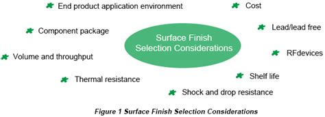
Benefits of ENIPIG Surface Finish
ENIPIG offers several key advantages over other surface finish technologies, making it an attractive choice for a wide range of electronics applications.
Superior Solderability
One of the most significant benefits of ENIPIG is its excellent solderability. The thin immersion gold layer provides a clean, oxide-free surface that promotes strong and reliable solder joints. This enhanced solderability is particularly important for fine-pitch components and high-density PCB designs, where robust and consistent solder connections are critical.
Enhanced Corrosion Resistance
The combination of electroless nickel, immersion palladium, and immersion gold layers in ENIPIG provides superior corrosion resistance compared to other surface finishes. The nickel layer acts as a barrier against copper diffusion, while the palladium and gold layers protect the nickel from oxidation and corrosion. This multi-layer protection ensures that the PCB remains stable and reliable, even in harsh environmental conditions.
Improved Durability
ENIPIG’s unique layered structure also contributes to its enhanced durability. The electroless nickel layer provides a hard, wear-resistant surface that can withstand the stresses of multiple reflow cycles and physical handling. The palladium layer acts as a barrier, preventing the formation of brittle intermetallic compounds between the nickel and gold layers, which can lead to solder joint failure. This improved durability extends the lifespan of the PCB and reduces the risk of field failures.
Compatibility with Lead-Free Soldering
As the electronics industry moves towards lead-free soldering to comply with environmental regulations, ENIPIG has emerged as a compatible and reliable surface finish option. The immersion gold layer provides excellent solderability with lead-free solder alloys, such as SAC305 (Sn96.5Ag3.0Cu0.5), ensuring strong and stable solder joints. Additionally, the high melting point of palladium (1828°C) prevents the formation of brittle intermetallic compounds during lead-free soldering processes, which typically require higher reflow temperatures.
Extended Shelf Life
ENIPIG-finished PCBs have a significantly longer shelf life compared to boards with other surface finishes. The immersion gold layer provides a stable, oxide-free surface that resists tarnishing and degradation over time. This extended shelf life is particularly beneficial for PCBs that may be stored for long periods before assembly or for applications where long-term reliability is crucial.

Applications of ENIPIG Surface Finish
The superior performance and reliability of ENIPIG make it suitable for a wide range of electronics applications, particularly those that demand high-reliability and durability.
Automotive Electronics
ENIPIG is increasingly used in automotive electronics due to its excellent corrosion resistance and compatibility with lead-free soldering processes. Automotive PCBs are often exposed to harsh environmental conditions, such as extreme temperatures, humidity, and vibration. The enhanced durability and stability of ENIPIG ensure that these PCBs can withstand these challenges and maintain reliable performance over the vehicle’s lifespan.
Aerospace and Defense
In the aerospace and defense industries, PCBs must meet stringent reliability and performance requirements. ENIPIG’s superior solderability, corrosion resistance, and durability make it an ideal choice for these demanding applications. The extended shelf life of ENIPIG-finished PCBs also benefits aerospace and defense projects, which often have longer development and production timelines.
Medical Devices
Medical devices require PCBs that can provide reliable performance and withstand the rigors of sterilization processes. ENIPIG’s excellent corrosion resistance and durability make it a suitable choice for medical electronics. The biocompatibility of the gold layer also makes ENIPIG an attractive option for implantable devices and other medical applications where biocompatibility is essential.
High-Density Interconnects (HDI)
HDI PCBs feature fine-pitch components and high-density layouts that demand superior solderability and reliability. ENIPIG’s thin immersion gold layer promotes strong, reliable solder joints, even with fine-pitch components. The enhanced durability of ENIPIG also ensures that HDI PCBs can withstand multiple reflow cycles and maintain their integrity over time.
Industrial Electronics
Industrial electronics often operate in harsh environments, exposed to high temperatures, humidity, and corrosive chemicals. ENIPIG’s multi-layer protection provides excellent corrosion resistance, making it a suitable choice for industrial PCBs. The enhanced durability of ENIPIG also ensures that these PCBs can withstand the rigors of industrial applications and maintain reliable performance over an extended lifespan.

ENIPIG vs. Other Surface Finishes
When considering surface finish options for PCBs, it is essential to compare ENIPIG with other popular finishes to understand their relative strengths and weaknesses.
ENIG (Electroless Nickel Immersion Gold)
ENIG is a widely used surface finish that consists of an electroless nickel layer followed by an immersion gold layer. While ENIG offers good solderability and corrosion resistance, it has some limitations compared to ENIPIG:
- ENIG is more prone to “black pad” syndrome, a defect characterized by the formation of brittle intermetallic compounds that can lead to solder joint failure.
- The gold layer in ENIG is thicker than in ENIPIG, which can lead to slower wetting times during soldering and potential issues with fine-pitch components.
ENEPIG (Electroless Nickel Electroless Palladium Immersion Gold)
ENEPIG is another advanced surface finish that shares similarities with ENIPIG. The key difference is that ENEPIG uses an electroless palladium layer instead of an immersion palladium layer. While ENEPIG offers comparable performance to ENIPIG, it has some drawbacks:
- The electroless palladium process in ENEPIG is more complex and expensive than the immersion palladium process in ENIPIG.
- The thicker palladium layer in ENEPIG can lead to slower wetting times during soldering compared to ENIPIG.
OSP (Organic Solderability Preservative)
OSP is a simple and cost-effective surface finish that involves applying an organic compound to the copper surface of the PCB. While OSP is a popular choice for low-cost applications, it has several limitations compared to ENIPIG:
- OSP has a shorter shelf life than ENIPIG, as the organic coating can degrade over time.
- The solderability of OSP-finished PCBs is not as consistent as ENIPIG, particularly after multiple reflow cycles.
- OSP provides limited protection against corrosion compared to the multi-layer protection of ENIPIG.

Implementing ENIPIG Surface Finish
To successfully implement ENIPIG surface finish in PCB manufacturing, several key factors must be considered:
Process Control
Strict process control is essential to ensure the consistency and quality of the ENIPIG surface finish. This includes maintaining the proper composition and temperature of the chemical baths, controlling the immersion times for each layer, and regularly monitoring the thickness and uniformity of the deposited layers.
Equipment and Chemistry
Implementing ENIPIG requires specialized equipment and chemistry. The chemical baths for electroless nickel, immersion palladium, and immersion gold must be carefully formulated and maintained to ensure optimal performance. The plating equipment must be designed to handle the specific requirements of the ENIPIG process, such as precise temperature control and efficient rinsing between steps.
Quality Control
Rigorous quality control measures must be in place to verify the integrity and performance of ENIPIG-finished PCBs. This includes visual inspections, thickness measurements, solderability testing, and cross-sectional analysis. Regular quality control checks help identify and address any issues in the ENIPIG process, ensuring that the finished PCBs meet the required specifications and performance standards.
Collaboration with Suppliers
Successful implementation of ENIPIG also requires close collaboration with suppliers of chemicals, equipment, and materials. Partnering with reputable and experienced suppliers can provide access to high-quality products, technical support, and process expertise. This collaboration helps ensure that the ENIPIG process is optimized for the specific requirements of the PCB manufacturer and end-use applications.
FAQ
-
Q: What is the typical shelf life of ENIPIG-finished PCBs?
A: ENIPIG-finished PCBs have an extended shelf life compared to other surface finishes. With proper storage conditions, ENIPIG-finished boards can maintain their solderability and performance for up to 12 months or more. -
Q: Is ENIPIG suitable for both lead-free and leaded soldering processes?
A: Yes, ENIPIG is compatible with both lead-free and leaded soldering processes. The immersion gold layer provides excellent solderability with various solder alloys, while the palladium layer prevents the formation of brittle intermetallic compounds during soldering. -
Q: How does ENIPIG compare to ENIG in terms of cost?
A: ENIPIG is generally more expensive than ENIG due to the additional palladium layer and the more complex process involved. However, the superior performance and reliability of ENIPIG often justify the increased cost for high-reliability applications. -
Q: Can ENIPIG be used for press-fit connectors?
A: Yes, ENIPIG is suitable for use with press-fit connectors. The hard, wear-resistant nickel layer provides a robust surface for the mechanical connection, while the gold layer enhances the electrical conductivity and corrosion resistance of the contact surface. -
Q: Is ENIPIG a RoHS-compliant surface finish?
A: Yes, ENIPIG is a RoHS-compliant surface finish. The materials used in the ENIPIG process, including nickel, palladium, and gold, are not restricted under the RoHS directive. Additionally, ENIPIG’s compatibility with lead-free soldering processes makes it an attractive choice for RoHS-compliant electronics manufacturing.
Conclusion
ENIPIG surface finish is a cutting-edge technology that offers superior performance, reliability, and durability compared to traditional surface finishes. With its excellent solderability, enhanced corrosion resistance, and compatibility with lead-free soldering processes, ENIPIG has become an increasingly popular choice for a wide range of electronics applications, including automotive, aerospace, medical, and industrial systems.
As the demand for high-reliability electronics continues to grow, the adoption of ENIPIG surface finish is expected to increase. PCB manufacturers that invest in implementing ENIPIG can differentiate themselves by offering a high-quality, reliable surface finish that meets the evolving needs of their customers.
However, successful implementation of ENIPIG requires careful consideration of process control, equipment, chemistry, and quality control measures. Close collaboration with suppliers and a commitment to continuous improvement are also essential for optimizing the ENIPIG process and ensuring consistent, high-quality results.
By embracing the benefits of ENIPIG surface finish and dedicating resources to its successful implementation, PCB manufacturers can position themselves at the forefront of the electronics industry, delivering innovative, reliable, and durable solutions to their customers.


Leave a Reply