Introduction
Printed circuit boards (PCBs) form the backbone of most modern electronic devices. From smartphones to TVs to computers, PCBs provide the platform to mount and connect electronic components using conductive copper traces. As electronic devices become more complex and packed with features, PCBs too have evolved to accommodate more components and connections in a small footprint. This evolution has led to the development of multilayer PCBs, with dual layer PCBs being the simplest and most common type of multilayer boards.
In this comprehensive guide, we will explore what dual layer PCBs are, their construction, pros and cons, design considerations, and application areas.
What are Dual Layer PCBs?
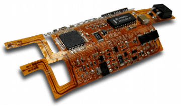
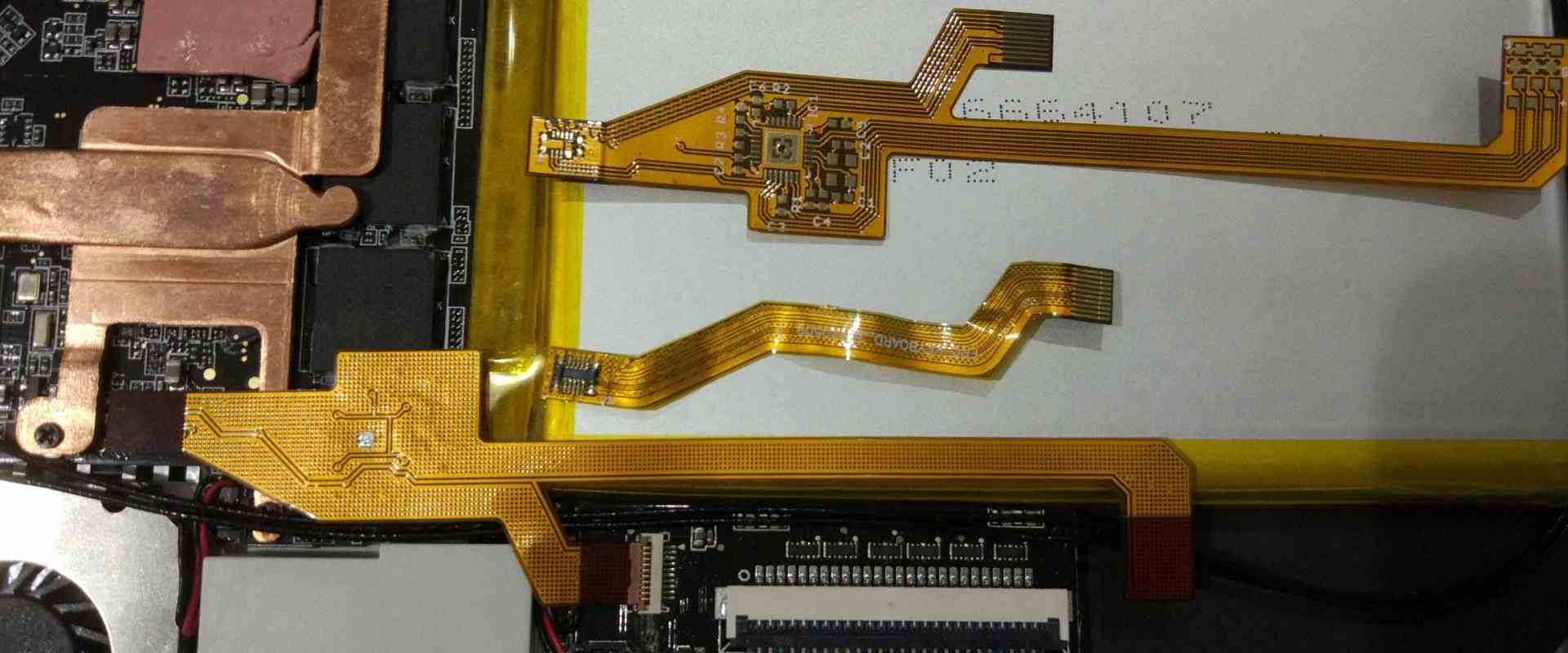
Dual layer PCBs contain two conductive copper layers separated by a dielectric substrate layer. The substrate layer acts as an insulator between the two copper layers. The components and devices are mounted on the top side of the PCB, while the bottom side contains the copper traces to connect the components according to the circuit design.
The key characteristics of dual layer PCBs are:
- Two layers of copper – top and bottom
- Substrate dielectric layer in between
- Components mounted on top side
- Traces and routes on bottom side
- Plated through holes connect top and bottom layers
Some key terms used in dual layer PCBs:
- Top layer – Where components are mounted. May contain some traces.
- Bottom layer – Dedicated for routing copper traces to connect components.
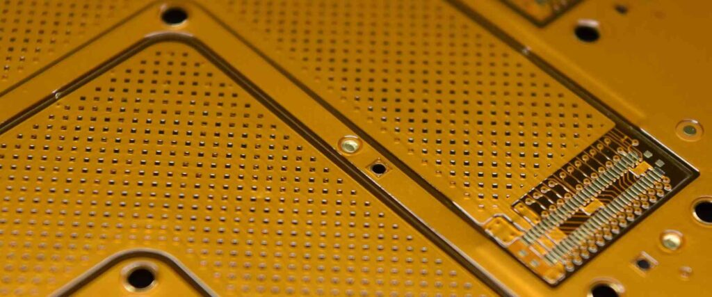
- Dielectric layer – Insulating substrate between top and bottom layers. Popular materials used are FR-4 and polyimide.
- Plated through hole (PTH) – Holes drilled through all layers to connect top and bottom layers electrically using copper plating.
- Via – A vertical interconnect between layers passing through dielectric substrate.
- Track/Trace – Horizontal copper interconnects on each signal layer.
- Pad – The termination point on a PCB for mounting and connecting a component.
Why Use Dual Layer PCBs?
Here are some of the key benefits of using dual layer PCBs:
1. Cost Effective
Dual layer boards provide a cost-effective solution compared to 4-layer and higher layer count PCBs. They require less complex fabrication processes, fewer materials, and minimum drilling operations. This makes them ideal for small to medium complexity designs that don’t require very dense routing.
2. Easy to Manufacture
The simple 2-layer construction of these boards reduces manufacturing complexity and cost. This makes dual layer PCBs ideal for small-scale production runs.
3. Flexible Routing
With access to two layers, routing of connections is more flexible compared to single-sided boards. Dual layer boards can accommodate moderately complex routing requirements.
4. Widely Supported
Most PCB manufacturers provide dual layer boards as their standard offering. The designs are highly supported across CAD tools and fabrication processes.
5. Easy Troubleshooting
With only two layers, it becomes easier to debug and troubleshoot designs. Internal layers make debugging much more complex.
6. Lightweight
Dual layer boards offer a lightweight solution due to simpler construction and fewer layers/materials. This makes them suitable for weight-sensitive applications like mobile devices.
In summary, dual layer PCBs provide the best balance of affordability, manufacturability, and routing flexibility for small to medium complexity designs.
Construction and Materials
The construction of a dual layer PCB involves the following steps:
- Substrate Material Selection – Popular options are FR-4 (glass reinforced epoxy), polyimide, Rogers, etc. Key considerations are dielectric constant, loss tangent, thermal conductivity and Z-axis expansion.
- Layer Stackup – Determines the order of conductive copper and dielectric layers. For dual layer, it’s copper-dielectric-copper. The dielectric thickness is typically 1.6mm.
- Copper Foil Selection – 1oz (35μm) copper foil is standard. Thicker foils are used for high current designs.
- Lamination – Individual layers are stacked up and laminated using high pressure and temperature. This bonds the layers together.
- Drilling – Holes are drilled for component holes, vias and for fastening. Min hole size is typically 0.3mm.
- Plating – Walls of drilled holes are plated with copper to create electrical interconnects between layers.
- Soldermask Application – A layer of epoxy soldermask is applied to protect copper traces from oxidation and shorting.
- Silkscreen Printing – White epoxy layer is printed to indicate component designators, polarity markings etc.
- Surface Finish – Immersion silver, ENIG, HASL are used to protect exposed copper from corrosion.
- Electrical Testing – Bare boards are tested for shorts, opens and impedance before component assembly.
Pros and Cons of Dual Layer PCBs
Pros
- Cost effective
- Easy to manufacture
- Flexible routing with two layers
- Wide industry support
- Easy debugging and testing
- Lightweight construction
Cons
- Limited routing capability compared to 4+ layer boards
- Not suitable for high component density designs
- Prone to EMI/noise pickup due to lack of ground plane
- Relatively lower signal speeds compared to multilayer boards
- Not suitable for high frequency applications above 25GHz
Design Considerations
Designing dual layer PCBs require certain considerations for layout, routing and DFM:
- Partitioning – Smartly partition the layout between top (components) and bottom (traces) layers. Group associated components.
- Routing – Use 45/90 degree angles. Route high speed traces over solid ground areas. Match trace widths to current requirements.
- Bypassing/Decoupling – Use dedicated power and ground traces. Provide local decoupling capacitors for each power section.
- Impedance Control – Match trace width and spacing to get 50/75/100 Ohm differential impedance for high speed traces.
- EMI Protection – Provide shielding, filtering and isolation for noise sensitive analog and digital sections.
- Thermal Management – Ensure adequate thermal relief vias and airflow for cooling high power components.
- Manufacturability – Follow design rules. Allow adequate spacing between traces, pads and components.
- Testability – Include testpoints, vias and ground pins for easy testing and debugging.
Smart component placement, routing and DFM techniques are key to designing reliable, high-performance dual layer PCBs.
Application Areas
Here are some of the popular application areas where dual layer PCBs provide the right balance of capability and cost:
- Consumer Electronics – Simple wearable devices, Bluetooth speakers, IoT products.
- Industrial Controls – Sensors, meters, controllers, data acquisition boards.
- Automotive – Instrument clusters, basic infotainment systems, LED lighting.
- Medical – Diagnostic instruments, patient monitoring devices.
- Avionics – Lighting controls, basic instrument panels, seat electronics.
- Communication – Low to medium complexity switchboards, routers, modems.
Overall, dual layer boards are the workhorses of the electronics industry and find use in a wide range of products where cost and reliability are important. The growth of smart devices for automation, IoT and transportation will further fuel the demand for these popular PCBs.
Dual Layer PCB Design Software
To efficiently design and lay out dual layer PCBs, ECAD software with the following features is recommended:
- Intelligent component placement
- Interactive routing with DRC
- Impedance and phase tuning
- Copper balancing and fill
- Thermal analysis
- 3D modelling
- Photorealistic rendering
- Libraries for common components
- Manufacturing/DFM rule checks
- Integration with PCB fabrication
Leading desktop ECAD options are Altium Designer, Cadence Allegro, and Mentor Xpedition. Popular cloud-based tools are Upverter, EasyEDA, and CircuitMaker.
ECAD software streamlines the PCB design process and allows engineers to design complex dual layer boards faster and with lower errors.
Dual Layer PCBs – Frequently Asked Questions
Here are some common queries regarding dual layer PCBs:
Q1. What is the typical thickness of the dielectric layer in dual layer PCBs?
The typical thickness of the dielectric substrate (e.g. FR4) in dual layer PCBs ranges from 0.8 mm to 1.6 mm. High frequency boards tend to use thinner dielectrics around 0.8mm while thicker 1.6mm dielectrics provide better structural rigidity.
Q2. What are the typical trace/track widths used on dual layer boards?
Common trace widths are:
- High current power traces: >70mil (>1.8mm)
- Default signal traces: 10mil (0.25mm)
- High speed signals: 6-8mil (0.15 – 0.2mm)
- Thin lines: 4mil (0.1mm)
Wider tracks are used for traces carrying higher currents as per current density limits.
Q3. What is the typical number of routing layers used on a 2-layer board?
Dual layer boards typically utilize both layers for routing – the top layer is used for short connections while the bottom layer handles most of the complex routing. A partial ground plane can sometimes be created on the top layer.
Q4. How are vias constructed in dual layer PCBs?
On dual layer boards, vias consist of plated through holes that connect the top and bottom copper layers. The via barrels are plated with 1oz copper to provide electrical connectivity. The minimum via diameter is typically 12mil.
Q5. What panel sizes are commonly used for dual layer PCB fabrication?
Common panel sizes are:
- 200mm x 100mm
- 200mm x 160mm
- 250mm x 160mm
- 300mm x 200mm
The panel is populated with multiple PCB designs to maximize fabrication efficiency.
Conclusion
Dual layer printed circuit boards offer the ideal balance of capability, reliability and cost for small to medium complexity electronic designs. With two conductive copper layers for routing, they provide sufficient flexibility for implementing a wide range of analog, digital, and mixed signal circuits.
Understanding the construction, advantages, design considerations and applications of dual layer PCB technology allows engineers to make the right choice while designing the core platform for electronics. With their versatile use across industries and given the continuing explosion of new electronics products, dual layer PCBs will remain the workhorse of the industry for the foreseeable future.


Leave a Reply