Introduction to PCB Design for IoT Devices
The Internet of Things (IoT) is revolutionizing how we interact with technology in our everyday lives. From smart homes and wearables to industrial automation and connected vehicles, IoT devices are becoming increasingly prevalent. At the heart of every IoT device lies a printed circuit board (PCB) that enables its functionality, connectivity, and performance. Designing PCBs for IoT applications requires careful consideration of various factors such as size, power consumption, wireless connectivity, sensor integration, and security. In this article, we will explore the key aspects of PCB design for IoT and provide insights into best practices and emerging trends.
Understanding the Unique Requirements of IoT PCB Design
Size and Form Factor Considerations
One of the primary challenges in designing PCBs for IoT devices is minimizing the size and optimizing the form factor. Many IoT applications require compact and lightweight devices that can be easily integrated into various environments. This necessitates the use of smaller components, higher density layouts, and creative packaging solutions. Some key considerations for size and form factor optimization include:
- Selecting smaller package sizes for components (e.g., chip-scale packages, quad-flat no-leads)
- Utilizing multi-layer PCBs to increase component density and reduce overall board size
- Implementing flexible or Rigid-flex PCBs for wearable and space-constrained applications
- Exploring 3D packaging techniques such as package-on-package (PoP) and system-in-package (SiP)
| Component Package | Size (mm) | Advantages |
|---|---|---|
| QFN (Quad-Flat No-Leads) | 2×2 to 12×12 | Reduced footprint, excellent thermal performance |
| BGA (Ball Grid Array) | 5×5 to 50×50 | High pin count, good thermal and electrical performance |
| CSP (Chip-Scale Package) | 0.5×0.5 to 1.5×1.5 | Smallest size, minimized parasitics |
| DFN (Dual-Flat No-Leads) | 1×1 to 5×5 | Compact size, good thermal performance |
Power Management and Battery Life Optimization
IoT devices often rely on battery power or energy harvesting techniques to operate autonomously. Efficient power management is crucial to extend battery life and ensure reliable operation. PCB designers must carefully consider power requirements and implement appropriate power management strategies. Some key aspects of power management in IoT PCB design include:
- Selecting low-power components and optimizing their operating conditions
- Implementing power gating techniques to selectively power down unused circuits
- Utilizing DC-DC converters and Voltage Regulators for efficient power conversion
- Designing for low quiescent current consumption and minimizing leakage currents
- Incorporating energy harvesting techniques such as solar, RF, or piezoelectric
Wireless Connectivity and Antenna Design
Wireless connectivity is a fundamental requirement for most IoT devices, enabling them to communicate with other devices, gateways, and cloud platforms. PCB designers must integrate appropriate wireless modules and design antennas that provide reliable and efficient wireless performance. Some common wireless technologies used in IoT include:
- Wi-Fi (802.11 b/g/n/ac)
- Bluetooth Low Energy (BLE)
- Zigbee
- LoRaWAN
- NB-IoT and LTE-M
Antenna design is a critical aspect of wireless performance in IoT devices. PCB designers must consider factors such as antenna type, placement, and impedance matching to ensure optimal wireless range and reliability. Some popular antenna types for IoT PCBs include:
- Printed antennas (e.g., meandered, inverted-F, monopole)
- Chip antennas
- External antennas (e.g., dipole, whip)
| Wireless Technology | Frequency | Range | Power Consumption |
|---|---|---|---|
| Wi-Fi | 2.4 GHz, 5 GHz | 50-100 m | Medium to High |
| Bluetooth Low Energy | 2.4 GHz | 10-100 m | Very Low |
| Zigbee | 2.4 GHz, 915 MHz, 868 MHz | 10-100 m | Low |
| LoRaWAN | 915 MHz, 868 MHz | 2-15 km | Very Low |
| NB-IoT and LTE-M | Licensed LTE bands | 1-10 km | Low |
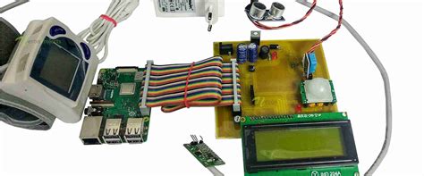
Sensor Integration and Signal Conditioning
IoT devices often rely on various sensors to gather data from their environment, such as temperature, humidity, motion, light, and pressure. Integrating these sensors onto the PCB requires careful consideration of signal conditioning, analog-to-digital conversion, and interface protocols. Some key aspects of sensor integration in IoT PCB design include:
- Selecting appropriate sensors based on accuracy, resolution, and power consumption requirements
- Designing signal conditioning circuits to amplify, filter, and process sensor signals
- Implementing analog-to-digital converters (ADCs) with suitable resolution and sampling rates
- Choosing appropriate interface protocols (e.g., I2C, SPI, UART) for sensor communication
- Considering sensor placement and shielding to minimize noise and interference
Security and Tamper Protection
IoT devices often handle sensitive data and operate in critical environments, making security a paramount concern. PCB designers must incorporate security features to protect against unauthorized access, tampering, and reverse engineering. Some key security considerations in IoT PCB design include:
- Implementing secure boot and firmware authentication mechanisms
- Utilizing hardware-based encryption engines for data protection
- Designing tamper-evident and tamper-resistant enclosures
- Implementing secure debug interfaces and disabling unnecessary ports
- Considering physical unclonable functions (PUFs) for device authentication

Best Practices for IoT PCB Design
Schematic Design and Component Selection
A well-designed schematic is the foundation of a successful IoT PCB. Some best practices for schematic design and component selection include:
- Use hierarchical design to organize complex schematics into logical blocks
- Follow consistent naming conventions and labeling for clarity and readability
- Select components based on performance, power consumption, and availability
- Use reliable and trusted component suppliers to ensure quality and authenticity
- Perform thorough design reviews and simulate critical circuits before layout
PCB Layout and Routing Techniques
Proper PCB layout and routing are essential for optimizing signal integrity, power distribution, and electromagnetic compatibility (EMC) in IoT devices. Some best practices for PCB layout and routing include:
- Follow manufacturer’s layout guidelines for critical components (e.g., wireless modules, antennas)
- Use appropriate trace widths and spacing based on signal requirements and PCB manufacturing capabilities
- Implement proper grounding techniques, such as ground planes and star grounding, to minimize noise and interference
- Route sensitive signals (e.g., high-speed, analog) away from noisy sources and provide adequate shielding
- Optimize component placement for short signal paths and efficient power distribution
Thermal Management and Heat Dissipation
Thermal management is crucial for ensuring the reliability and longevity of IoT devices, especially in compact form factors. Some best practices for thermal management in IoT PCB design include:
- Identify heat-generating components and provide adequate thermal relief (e.g., copper pours, thermal vias)
- Use thermal interface materials (TIMs) and heatsinks for efficient heat dissipation
- Consider the use of thermal simulation tools to analyze and optimize thermal performance
- Design for appropriate airflow and ventilation in the device enclosure
- Monitor and control temperature using on-board sensors and software algorithms
EMC and Regulatory Compliance
IoT devices must comply with various electromagnetic compatibility (EMC) and regulatory standards to ensure safe and reliable operation. Some key considerations for EMC and regulatory compliance in IoT PCB design include:
- Understand the applicable standards and regulations for the target market and application (e.g., FCC, CE, IC)
- Implement proper EMI suppression techniques, such as filtering, shielding, and grounding
- Use appropriate ESD protection devices to safeguard sensitive components
- Conduct pre-compliance testing to identify and resolve EMC issues early in the design process
- Maintain proper documentation and certification for regulatory approvals

Emerging Trends and Future Directions
Flexible and Stretchable Electronics
Flexible and stretchable electronics are gaining traction in IoT applications, particularly in wearables and biomedical devices. These technologies enable conformable and ergonomic form factors that can adapt to various surfaces and movements. Some emerging trends in flexible and stretchable electronics for IoT include:
- Printed electronics using conductive inks and flexible substrates
- Stretchable interconnects and elastomeric materials for enhanced durability
- Integration of flexible sensors and energy harvesting components
- Advanced packaging techniques for encapsulation and protection
Edge Computing and AI Integration
Edge computing and artificial intelligence (AI) are transforming the way IoT devices process and analyze data. By moving computation closer to the source of data, edge computing enables real-time decision-making, reduced latency, and improved privacy. AI integration allows IoT devices to learn and adapt to their environment, enabling intelligent automation and predictive maintenance. Some key trends in edge computing and AI for IoT PCB design include:
- Integration of powerful microcontrollers and system-on-chip (SoC) solutions for edge processing
- Incorporation of dedicated AI accelerators and neural processing units (NPUs)
- Optimization of power consumption and thermal management for AI workloads
- Development of lightweight AI models and algorithms for resource-constrained devices
Modular and Configurable PCB Design
Modular and configurable PCB design approaches are gaining popularity in IoT development, allowing for faster time-to-market and increased flexibility. By designing PCBs with modular components and interfaces, developers can easily customize and upgrade IoT devices to meet specific application requirements. Some benefits of modular and configurable PCB design include:
- Reduced development time and costs by reusing common modules and components
- Ability to adapt to changing market demands and technological advancements
- Simplified maintenance and repair through module replacement
- Facilitation of product line expansion and customization

Frequently Asked Questions (FAQ)
- What are the key considerations for selecting wireless connectivity options for IoT PCBs?
-
When selecting wireless connectivity options for IoT PCBs, consider factors such as range, power consumption, data rate, security, and compatibility with existing infrastructure. Evaluate the specific requirements of your application and choose the most suitable wireless technology, such as Wi-Fi, Bluetooth Low Energy, Zigbee, or LPWAN protocols like LoRaWAN or NB-IoT.
-
How can I optimize power consumption in my IoT PCB design?
-
To optimize power consumption in your IoT PCB design, consider the following techniques:
- Select low-power components and optimize their operating conditions
- Implement power gating and sleep modes to selectively power down unused circuits
- Use efficient power conversion and voltage regulation techniques
- Minimize leakage currents and optimize for low quiescent current consumption
- Explore energy harvesting techniques to supplement battery power
-
What are some best practices for integrating sensors into IoT PCBs?
-
When integrating sensors into IoT PCBs, follow these best practices:
- Choose sensors based on accuracy, resolution, and power consumption requirements
- Design appropriate signal conditioning circuits for amplification, filtering, and processing
- Select suitable analog-to-digital converters (ADCs) with adequate resolution and sampling rates
- Use appropriate interface protocols (e.g., I2C, SPI, UART) for sensor communication
- Consider sensor placement and shielding to minimize noise and interference
-
How can I ensure the security and tamper protection of my IoT PCB?
-
To ensure the security and tamper protection of your IoT PCB, consider implementing the following measures:
- Use secure boot and firmware authentication mechanisms
- Incorporate hardware-based encryption engines for data protection
- Design tamper-evident and tamper-resistant enclosures
- Implement secure debug interfaces and disable unnecessary ports
- Explore the use of physical unclonable functions (PUFs) for device authentication
-
What are some emerging trends in IoT PCB design?
- Some emerging trends in IoT PCB design include:
- Flexible and stretchable electronics for wearables and biomedical applications
- Edge computing and AI integration for real-time data processing and intelligent automation
- Modular and configurable PCB design approaches for faster development and customization
- Advanced packaging techniques like system-in-package (SiP) and 3D packaging for compact form factors
- Incorporation of energy harvesting technologies for self-powered IoT devices
Conclusion
Designing PCBs for the Internet of Things requires a multidisciplinary approach that takes into account the unique requirements of IoT applications. From size and power optimization to wireless connectivity and sensor integration, PCB designers must navigate a complex landscape of design challenges and trade-offs. By following best practices in schematic design, component selection, PCB layout, and thermal management, designers can create robust and reliable IoT devices that meet the demands of an increasingly connected world.
As the IoT ecosystem continues to evolve, emerging trends such as flexible electronics, edge computing, AI integration, and modular design approaches will shape the future of IoT PCB design. By staying abreast of these developments and adopting innovative design strategies, PCB designers can unlock new possibilities and drive the growth of the Internet of Things.


Leave a Reply