Introduction
Flexible printed circuit boards (PCBs) represent an important enabling technology for modern electronic devices that require flexible form factors. While rigid PCBs were historically dominant, flexible circuits are increasingly being used in consumer electronics, automotive systems, industrial equipment, and medical devices where bending, flexing, or twisting is required. Designing flexible PCBs poses unique challenges compared to rigid boards. This article provides an overview of best practices for designing flexible circuits to meet application requirements for flexibility, reliability, and manufacturability.
Flexible PCB Materials
Flexible PCBs are made from thin, flexible dielectric materials clad with conductive copper traces. Typical base materials include polyimide (PI or Kapton), polyethylene terephthalate (PET), polyethylene naphthalate (PEN), polyether ether ketone (PEEK), and polytetrafluoroethylene (PTFE or Teflon). Polyimide is most commonly used due to its thermal stability, chemical resistance, and mechanical properties.
Flexible PCB Dielectrics
| Material | Description | Key Properties |
|---|---|---|
| Polyimide | High-performance resin, amber/yellow colored | Excellent thermal stability, chemical resistance, dimensional stability, high tensile strength |
| PET | Clear plastic, low cost | Moderate flexibility, lower temp rating than polyimide |
| PEN | High-performance polyester, clear | Increased tensile strength, thermal stability vs. PET |
| PEEK | High-temp engineered plastic | Excellent thermal, chemical resistance; less flexible than polyimide |
| PTFE | Inert fluoropolymer, opaque off-white | Extreme chemical resistance; less flexible than other materials |
Coverlay and Bonding Films
In addition to the base dielectric, flexible PCBs often use coverlay materials laminated over the circuitry for insulation and protection. Common coverlay films include polyimide, PET, PEN or acrylic. Flexible adhesive films such as acrylic or epoxy are also used for multilayer board lamination.
Design Rules and Guidelines
Successfully designing a flexible PCB requires accounting for the unique constraints and requirements compared to rigid boards. Some key considerations include:
Flexibility
- Minimum bend radius – The smallest radius a flex circuit can be bent without damaging the traces or copper. Depends on stackup, materials, and copper thickness.
- Dynamic flexing – Some applications require continuous dynamic bending. May require specially tested base materials.
- Folding and twisting – May introduce additional stresses not seen in simple bends.
Reliability
- Adhesion strength – Delamination of flexible layers is a concern, especially for dynamic flexing. Proper treatment and adhesives are necessary.
- Environmental exposure – Flex circuits in consumer devices will experience greater mechanical and thermal stresses.
Assembly
- Component sizes and profiles – Low profile components allow tighter bends. Avoid tall components in bend areas.
- Component placement – Strategic placement is needed to avoid placing components in high stress areas.
- Stiffeners – Can be added to protect components, stabilize connectors, or reduce flex stresses.
Manufacturing
- Minimum trace/space – Fabrication capabilities limit the fineness of the circuits. Typical minimum trace/space is around 4/4 mil (0.1mm).
- Impedance control – Controlling trace impedance is more difficult due to flexible materials. Wider lines are often required.
- Plated through holes – Flexible boards often rely more on conductive adhesives rather than plated holes.
- Handling and carrier boards – Flex circuits require specialized handling to avoid damage before assembly. Stiffener boards can be used as carriers.
Recommended Design Rules
| Feature | Recommended |
|---|---|
| Minimum bend radius | 10x circuit thickness minimum |
| Pad size | 0.020″ (0.5mm) minimum |
| Component distance from bend | >= 3x circuit thickness |
| Coverlay overlap | 0.040″ (1mm) beyond pads |
| Conductor width | 0.003″ (0.076mm) minimum |
| Conductor spacing | 0.003″ (0.076mm) minimum |
Layout and Routing
Proper layout techniques are critical for a successful flexible PCB design. The placement of components and routing of traces should account for the bending and twisting requirements to avoid failure.
Component Placement
- Place components in neutral bend areas whenever possible
- Avoid placing components or vias in high stress locations
- Orient tall components perpendicular to bend axis
- Use adhesives, underfills, and clips to strengthen component attachments
Routing Traces
- Route traces perpendicular to bend axis to reduce flex stresses
- Avoid traces near the neutral axis where bending is maximum
- Use curved, serpentine traces instead of right angles
- Wider traces and spaces reduce strain versus fine features
- Minimize crossing split lines between rigid sections
Stiffeners and Spreader Bars
- Place stiffeners over components or connectors to reduce stresses
- Use stiffener adhesive over entire surface for maximum strength
- Spreader bars maintain minimum bend radius between rigid areas
Flex Cuts and Scoring
- Strategic cuts in the flex board create flexible hinges between rigid segments
- Cuts go fully through the dielectric but not conductors
- Should begin/end halfway through pads connected by plated holes
- Allow room for tear propagation past the cut ends
Examples of Flexible Circuits
There are many types of flexible circuit applications and configurations. Some common examples include:
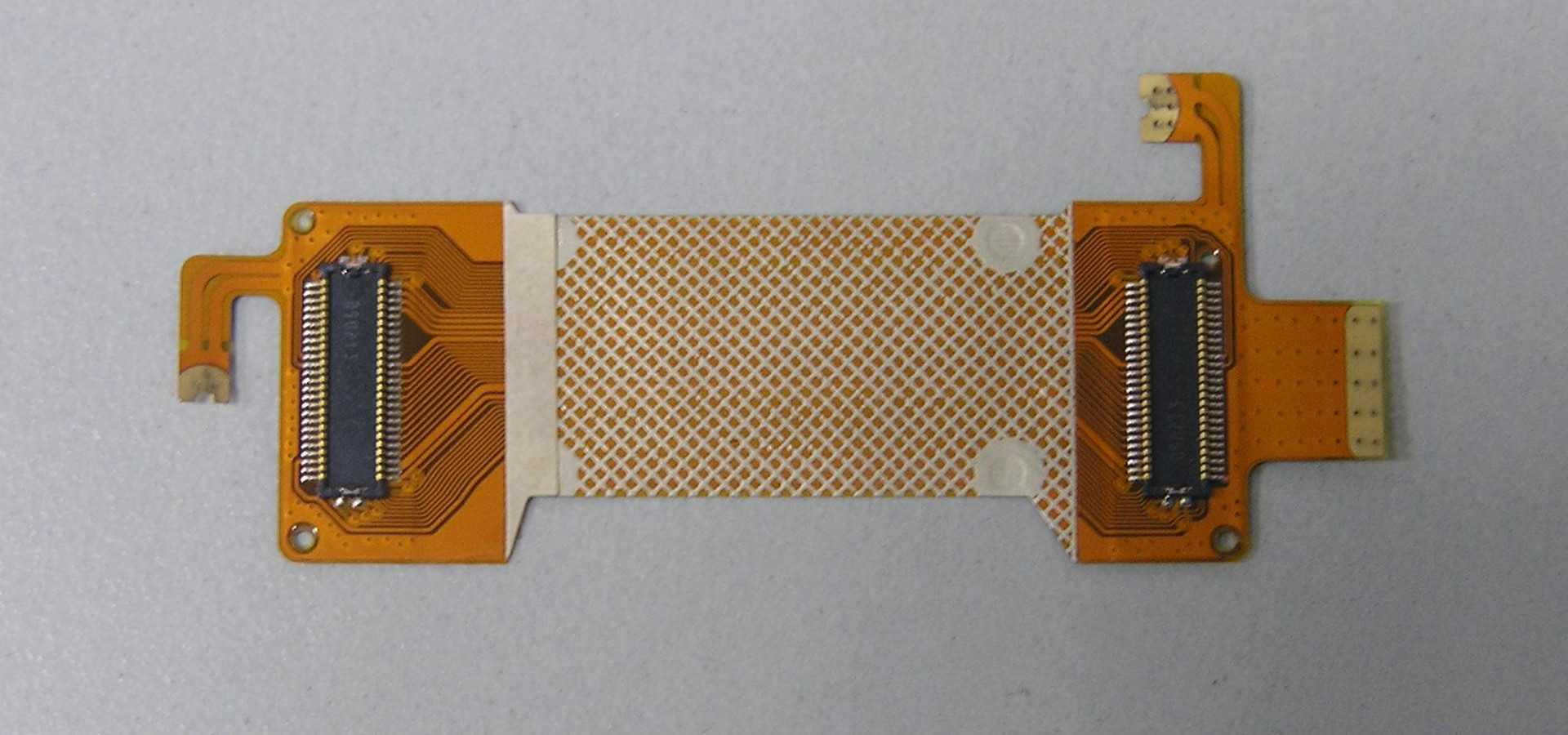
Flex-to-Board
A simple flex circuit extending from a rigid printed circuit board. Used for interconnections that require dynamic flexing or three-dimensional routing.
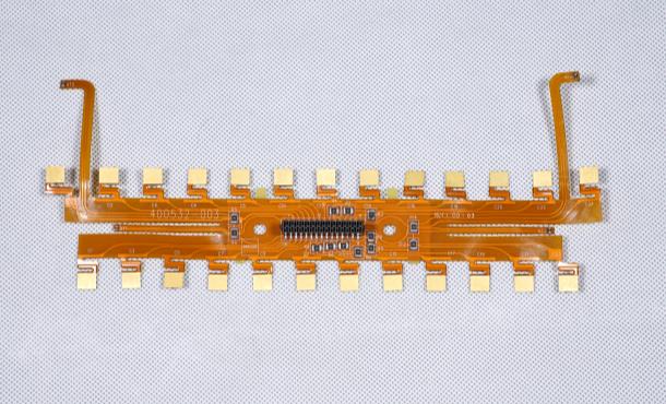
Flexible Cables
Interconnect cables made of multilayer flex circuits with high conductor counts. Often used as replacements for ribbon cables.
Flexible Displays
Thin circuits to support flexible displays. May have multilayer interconnects and mounted driver ICs.
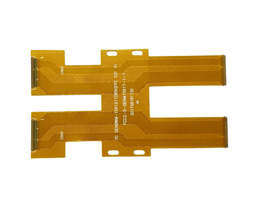
Flex-Rigid Combination
Combines rigid boards and flexible circuits all as one assembly. Rigid sections mount components while flex sections interconnect.
Prototyping and Testing
Validation through prototyping is important when working with flexible PCBs. Some tips include:
- Build multiple prototypes to test different bend radii, trace widths, adhesives etc.
- Perform cyclic flexing early to validate flexibility and reliability over product lifetime
- Use test boards with strain gages or finite element analysis to characterize stresses
- Ensure assembly process, components, and connectors are compatible with any flexing or handling required
Conclusion
Flexible PCBs provide unique advantages for interconnectivity and packaging in modern electronic devices. However, considering flexibility requirements throughout the design process is essential to ensuring reliable performance. Following the guidelines and best practices outlined here will set flexible PCB designs up for success.
Frequently Asked Questions
Q: What are some typical applications for flexible PCBs?
A: Flexible PCBs are widely used in consumer electronics (phones, wearables, displays), automotive applications (sensors, cameras, engine systems), medical devices (implants, catheters), industrial equipment (robotics, factory automation), and aerospace systems. Any application where a rigid board would be unfeasible.
Q: How do flexible PCBs achieve conductivity between layers?
A: Flexible multilayer boards rely more on conductive adhesives instead of plated through holes. Adhesives like anisotropic conductive films (ACF) provide conductivity when compressed between layers. Some flexible boards may use plated through holes with annular ring patterns to relieve stresses.
Q: Are there limitations on component sizes and profiles for flexible PCBs?
A: Yes, low profile components work best for tight bend radii. Tall, large components should be avoided in bend areas as they create high stress points. Passives and small footprint ICs are ideal. Strategic stiffening can allow some larger components.
Q: Can flex PCBs incorporate controlled impedance transmission lines?
A: It is possible but more challenging than with rigid boards. Wider lines are usually required to compensate for material properties. Some key considerations are uniform dielectric thickness, laminate quality, and handling procedures.
Q: How are flexible PCB prototypes typically fabricated?
A: Many flex PCB manufacturers offer quick-turn prototyping services. Laminated Kapton sheets and adhesive films allow hand-assembly of multilayer prototypes. Laser etching can be used for circuitry instead of photolithographic processes.


Leave a Reply