Introduction to PCB Services
Printed circuit boards (PCBs) are essential components in virtually all modern electronic devices. PCB services encompass the design, fabrication, assembly, and testing of these boards to ensure they meet the required specifications and function properly in the end product. As technology advances and competition intensifies, businesses are constantly seeking ways to reduce costs without compromising on quality. This article explores various strategies and approaches to cost-cutting in PCB services while maintaining high standards of performance and reliability.
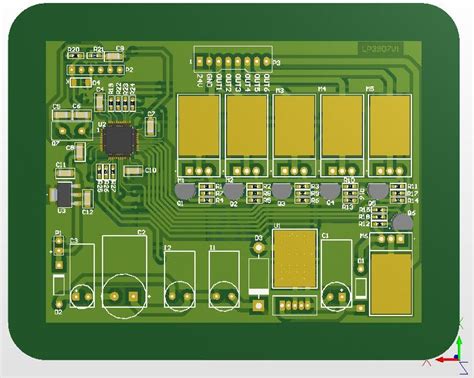
Understanding the PCB Manufacturing Process
To effectively implement cost-cutting measures in PCB services, it is crucial to have a thorough understanding of the PCB manufacturing process. The typical steps involved in PCB fabrication include:
-
Design and Layout: The PCB design is created using specialized software, taking into account the circuit requirements, component placement, and routing of traces.
-
Material Selection: The appropriate substrate material, typically FR-4, is chosen based on the application’s requirements, such as thermal stability, dielectric constant, and mechanical strength.
-
Printing and Etching: The circuit pattern is transferred onto the substrate using photolithography or screen printing techniques, followed by etching away the unwanted copper to form the traces.
-
Drilling and Plating: Holes are drilled through the board to accommodate through-hole components and vias. The holes are then plated with copper to establish electrical connections between layers.
-
Solder Mask and Silkscreen: A solder mask is applied to protect the copper traces from oxidation and prevent solder bridging. The silkscreen layer is added to provide component labels and other markings.
-
Surface Finishing: The exposed copper areas are coated with a protective finish, such as HASL (Hot Air Solder Leveling), ENIG (Electroless Nickel Immersion Gold), or OSP (Organic Solderability Preservative), to enhance solderability and prevent corrosion.
-
Electrical Testing: The fabricated PCBs undergo electrical testing to ensure they meet the specified requirements and are free from shorts, opens, and other defects.
By optimizing each step of the manufacturing process, PCB service providers can identify opportunities for cost reduction without compromising on quality.

Strategies for Cost-cutting in PCB Services
1. Design Optimization
One of the most effective ways to reduce PCB Manufacturing Costs is through design optimization. By carefully considering the following factors during the design phase, significant savings can be achieved:
a. Minimizing Board Size: Reducing the overall dimensions of the PCB can lead to material savings and increased panel utilization, resulting in lower production costs.
b. Optimizing Layer Count: Striking a balance between the number of layers and the required functionality can help minimize fabrication costs. Avoiding unnecessary layers and utilizing efficient routing techniques can reduce complexity and manufacturing expenses.
c. Standardizing Components: Using standardized and readily available components instead of custom or obsolete parts can significantly reduce procurement costs and lead times.
d. Design for Manufacturing (DFM): Incorporating DFM principles, such as maintaining proper trace widths and clearances, avoiding acute angles, and providing adequate spacing between components, can improve manufacturability and yield, ultimately reducing costs.
2. Material Selection and Sourcing
Careful selection and sourcing of materials can have a significant impact on PCB manufacturing costs. Consider the following approaches:
a. Volume Pricing: Negotiating volume discounts with material suppliers can lead to significant cost savings, especially for high-volume production runs.
b. Alternative Materials: Exploring alternative substrate materials, such as high-Tg FR-4 or halogen-free laminates, can offer cost benefits without compromising performance.
c. Supplier Consolidation: Consolidating purchases with fewer suppliers can streamline logistics, reduce transaction costs, and provide opportunities for better pricing through long-term partnerships.
3. Process Optimization and Automation
Streamlining the PCB manufacturing process through optimization and automation can contribute to cost reduction in several ways:
a. Lean Manufacturing: Implementing lean manufacturing principles, such as continuous improvement, waste reduction, and just-in-time inventory management, can minimize costs associated with inefficiencies and excess inventory.
b. Automated Inspection: Investing in automated optical inspection (AOI) and automated x-ray inspection (AXI) systems can reduce manual inspection time, improve defect detection, and minimize rework costs.
c. Data-driven Decision Making: Utilizing manufacturing execution systems (MES) and analytics tools to collect and analyze production data can help identify bottlenecks, optimize resource allocation, and make data-driven decisions for cost optimization.
4. Outsourcing and Strategic Partnerships
Outsourcing certain aspects of PCB services to specialized providers or forming strategic partnerships can lead to cost savings through economies of scale and access to advanced capabilities:
a. Fabrication Outsourcing: Partnering with offshore PCB fabrication facilities in regions with lower labor and overhead costs can significantly reduce manufacturing expenses, especially for high-volume production.
b. Assembly Outsourcing: Outsourcing PCB Assembly to specialized service providers with automated assembly lines and experienced technicians can minimize capital investments and achieve cost efficiencies.
c. Design Collaboration: Collaborating with design partners or utilizing third-party design services can access specialized expertise and advanced design tools without the need for in-house investments.

Cost-cutting Case Studies
Case Study 1: Automotive Electronics Manufacturer
An automotive electronics manufacturer faced challenges in reducing PCB costs while maintaining strict quality and reliability standards. By implementing the following cost-cutting measures, the company achieved significant savings:
- Design optimization through component standardization and DFM principles
- Material sourcing strategies, including volume pricing and alternative substrates
- Process automation with AOI and MES implementation
- Strategic outsourcing of high-volume fabrication to a reliable offshore partner
As a result, the manufacturer reduced PCB costs by 25% without compromising on quality or delivery performance.
Case Study 2: Medical Device Startup
A medical device startup sought to minimize PCB costs to maximize its limited budget during product development. The company employed the following cost-cutting approaches:
- Iterative design optimization to minimize board size and layer count
- Utilization of open-source design tools and libraries
- Partnering with a local PCB Prototyping service for quick-turn fabrication
- Outsourcing assembly to a specialized provider with experience in medical device manufacturing
Through these measures, the startup reduced its PCB development costs by 35% and accelerated time-to-market for its innovative medical device.

FAQ
1. How can I ensure the quality of my PCBs while cutting costs?
A: Implementing robust quality control measures, such as automated inspection and rigorous testing, can help maintain PCB Quality while pursuing cost-cutting initiatives. Additionally, partnering with reputable PCB service providers with a proven track record of quality and reliability can mitigate the risks associated with cost reduction.
2. What are the potential risks of outsourcing PCB fabrication to offshore facilities?
A: Offshore outsourcing can introduce risks such as longer lead times, communication challenges, and potential quality issues. To mitigate these risks, it is essential to thoroughly vet potential offshore partners, establish clear quality expectations, and maintain open communication channels throughout the manufacturing process.
3. How can I optimize my PCB design for cost reduction?
A: PCB design optimization for cost reduction involves techniques such as minimizing board size, optimizing layer count, standardizing components, and incorporating DFM principles. Collaborating with experienced PCB designers and utilizing advanced design tools can help identify cost-saving opportunities without compromising functionality or reliability.
4. What are the benefits of strategic partnerships in PCB services?
A: Strategic partnerships in PCB services can offer several benefits, including access to specialized expertise, advanced manufacturing capabilities, and cost efficiencies through economies of scale. By fostering long-term relationships with trusted partners, companies can achieve sustainable cost reductions and improve overall supply chain performance.
5. How can data analytics contribute to cost-cutting in PCB manufacturing?
A: Data analytics can provide valuable insights into PCB manufacturing processes, enabling data-driven decision-making for cost optimization. By collecting and analyzing production data, manufacturers can identify inefficiencies, optimize resource allocation, predict maintenance needs, and continuously improve processes to reduce costs and enhance productivity.
Conclusion
Cost-cutting in PCB services is a multifaceted endeavor that requires a holistic approach encompassing design optimization, material selection, process automation, and strategic partnerships. By understanding the intricacies of the PCB manufacturing process and implementing targeted cost reduction strategies, businesses can achieve significant savings without compromising on quality or performance.
However, it is crucial to strike a balance between cost reduction and long-term sustainability. Short-sighted cost-cutting measures that sacrifice quality, reliability, or customer satisfaction can lead to higher costs in the long run. Therefore, PCB service providers must carefully evaluate the trade-offs and prioritize initiatives that deliver sustainable cost benefits while maintaining the highest standards of excellence.
As technology continues to evolve and market demands shift, the PCB industry must remain agile and adaptable. By embracing innovation, fostering collaboration, and continuously seeking opportunities for improvement, PCB service providers can navigate the challenges of cost reduction and emerge as competitive leaders in the ever-changing landscape of Electronic Manufacturing.


Leave a Reply