Introduction to PCB Component Placement
Printed Circuit Board (PCB) component placement is a crucial step in the PCB Assembly process. It involves the precise positioning and orientation of electronic components onto the PCB substrate. The primary goal of component placement is to ensure optimal electrical performance, mechanical stability, and manufacturability of the PCB assembly.
The Importance of Proper PCB Component Placement
Proper PCB component placement is essential for several reasons:
-
Electrical Performance: Correct placement of components minimizes signal interference, crosstalk, and noise, leading to better electrical performance of the PCB.
-
Thermal Management: Strategically placing heat-generating components, such as power regulators and processors, allows for efficient heat dissipation and prevents thermal stress on nearby components.
-
Mechanical Stability: Appropriate component placement ensures that the PCB assembly can withstand mechanical stresses during handling, transportation, and operation.
-
Manufacturing Efficiency: Well-planned component placement facilitates automated assembly processes, reducing the likelihood of assembly errors and improving overall production efficiency.
Factors to Consider in PCB Component Placement
Several factors must be taken into account when determining the optimal placement of components on a PCB:
1. Electrical Considerations
- Signal Integrity: High-speed signals should be routed with minimal interference, and sensitive components should be placed away from noisy components.
- Power Distribution: Power components should be placed close to their respective loads to minimize voltage drops and ensure stable power delivery.
- Electromagnetic Compatibility (EMC): Proper placement of components can help minimize electromagnetic interference (EMI) and ensure compliance with EMC regulations.
2. Mechanical Considerations
- Component Size and Shape: The physical dimensions and packaging of components dictate their placement on the PCB.
- Mounting Requirements: Some components may require specific mounting techniques, such as through-hole or surface mount, which affects their placement.
- Mechanical Stresses: Components subject to high mechanical stresses, such as connectors and switches, should be placed in areas that minimize stress on the PCB.
3. Thermal Considerations
- Heat Generation: Heat-generating components should be placed in areas with adequate cooling, such as near heatsinks or airflow paths.
- Thermal Coupling: Components with similar thermal characteristics should be grouped together to minimize thermal gradients across the PCB.
4. Manufacturing Considerations
- Assembly Process: The placement of components should be optimized for the specific assembly process used, such as pick-and-place machines or manual assembly.
- Soldering Requirements: Components with different soldering requirements, such as reflow soldering or wave soldering, should be grouped accordingly.
- Testability: Components should be placed in a manner that facilitates testing and debugging of the PCB assembly.

PCB Component Placement Techniques
Several techniques can be employed to achieve optimal component placement on a PCB:
1. Functional Grouping
Components with related functions should be grouped together on the PCB. This approach simplifies routing, minimizes signal interference, and improves overall system performance. For example, analog and digital components should be separated to minimize noise coupling.
2. Placement by Height
Components should be placed on the PCB according to their height profile. Taller components, such as electrolytic capacitors and connectors, should be placed near the edges of the board to prevent shadowing during the soldering process. Shorter components can be placed closer to the center of the board.
3. Thermal Grouping
Components with similar thermal characteristics should be grouped together to minimize thermal gradients across the PCB. This technique is particularly important for power components and heat-sensitive devices. By placing these components in close proximity, heat can be efficiently dissipated through a shared heatsink or cooling mechanism.
4. Orientation and Alignment
The orientation and alignment of components play a significant role in PCB assembly and performance. Components should be oriented in a manner that facilitates easy soldering and minimizes the risk of tombstoning (when a component stands up on one end during soldering). Additionally, aligning components in a consistent direction improves readability and aids in manual assembly processes.
5. Placement for Testability
Components should be placed in a way that enables easy access for testing and debugging. Test points should be strategically located to allow for probing of critical signals without interfering with other components. Placing components in a logical and accessible manner simplifies troubleshooting and reduces the time required for testing and repairs.

PCB Component Placement Tools and Software
To aid in the component placement process, various tools and software solutions are available:
1. CAD Software
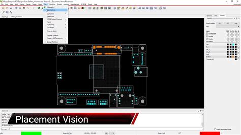
Computer-Aided Design (CAD) software, such as Altium Designer, Cadence Allegro, and KiCad, provides a comprehensive environment for PCB design and component placement. These tools offer features like 3D visualization, design rule checking (DRC), and automatic component placement based on predefined rules and constraints.
2. Placement Optimization Tools
Specialized placement optimization tools, such as Cadence Allegro PCB Placement Expert and Mentor Graphics Xpedition, use advanced algorithms to automatically place components on the PCB based on user-defined constraints and design rules. These tools can significantly reduce the time and effort required for manual component placement while ensuring optimal results.
3. Simulation and Analysis Tools
Simulation and analysis tools, like Ansys SIwave and Keysight ADS, allow designers to simulate the electrical and thermal behavior of the PCB assembly. These tools can help identify potential issues related to signal integrity, power distribution, and thermal management, enabling designers to make informed decisions about component placement.

Best Practices for PCB Component Placement
To ensure successful PCB component placement, consider the following best practices:
-
Define Placement Constraints: Clearly define placement constraints, such as component clearances, thermal requirements, and mechanical restrictions, before starting the placement process.
-
Prioritize Critical Components: Place critical components, such as high-speed devices, sensitive analog components, and power regulators, first to ensure optimal performance.
-
Minimize Signal Path Lengths: Place components to minimize the length of critical signal paths, reducing signal integrity issues and improving overall system performance.
-
Ensure Proper Grounding: Place components in a way that facilitates proper grounding and minimizes ground loops, which can cause noise and interference.
-
Consider Assembly and Manufacturing: Optimize component placement for the specific assembly and manufacturing processes used, ensuring compatibility with pick-and-place machines, soldering techniques, and testing requirements.
-
Perform Design Reviews: Regularly review the component placement with stakeholders, including electrical engineers, mechanical engineers, and manufacturing personnel, to identify and address any potential issues early in the design process.
Common PCB Component Placement Challenges and Solutions
PCB component placement can present various challenges that designers must address to ensure a successful PCB assembly. Some common challenges and their solutions include:
1. Limited Board Space
Challenge: Fitting all the required components within the available board space can be difficult, especially in compact or high-density designs.
Solution: Utilize smaller component packages, such as chip-scale packages (CSPs) or quad-flat no-leads (QFNs), and consider using multi-layer PCBs to accommodate more components and routing.
2. Thermal Management
Challenge: Ensuring proper thermal management for heat-generating components can be challenging, particularly in designs with limited board space or high power requirements.
Solution: Employ thermal simulation tools to identify potential hot spots and optimize component placement accordingly. Use thermal management techniques, such as heatsinks, thermal vias, and strategic component placement, to dissipate heat effectively.
3. Signal Integrity
Challenge: Maintaining signal integrity in high-speed designs can be difficult, as improper component placement can lead to crosstalk, reflections, and other signal quality issues.
Solution: Follow best practices for high-speed PCB design, such as minimizing signal path lengths, proper termination, and avoiding sharp bends in traces. Use simulation tools to analyze signal integrity and make necessary adjustments to component placement.
4. Manufacturing Constraints
Challenge: Ensuring compatibility with manufacturing processes and assembly equipment can be challenging, especially for designs with unique or non-standard component packages.
Solution: Collaborate closely with the manufacturing team to understand their capabilities and constraints. Design for manufacturability (DFM) by following guidelines for component placement, such as minimum clearances, orientation, and soldering requirements.
FAQ
1. What is the most important factor to consider when placing components on a PCB?
The most important factor to consider when placing components on a PCB depends on the specific design requirements. However, in general, ensuring proper electrical performance, thermal management, and manufacturability are the top priorities.
2. How can I minimize signal integrity issues through component placement?
To minimize signal integrity issues, place high-speed components close together to minimize signal path lengths, separate sensitive analog components from noisy digital components, and ensure proper grounding and termination.
3. What are some common PCB component placement mistakes to avoid?
Common PCB component placement mistakes include:
– Placing components too close together, leading to manufacturing difficulties and potential short circuits.
– Neglecting thermal management, resulting in overheating and reduced component lifespan.
– Ignoring signal integrity considerations, causing crosstalk, reflections, and other signal quality issues.
– Failing to consider manufacturing constraints, leading to assembly challenges and increased production costs.
4. How can I optimize component placement for automated assembly processes?
To optimize component placement for automated assembly processes, consider the following:
– Group components with similar heights and soldering requirements together.
– Ensure adequate clearances between components for pick-and-place machines.
– Orient components in a consistent direction to facilitate machine vision and placement accuracy.
– Provide sufficient space for solder paste application and reflow soldering.
5. What tools or software can help me with PCB component placement?
Several tools and software solutions can assist with PCB component placement, including:
– CAD software like Altium Designer, Cadence Allegro, and KiCad for design and component placement.
– Placement optimization tools like Cadence Allegro PCB Placement Expert and Mentor Graphics Xpedition for automated component placement.
– Simulation and analysis tools like Ansys SIwave and Keysight ADS for evaluating electrical and thermal performance.
Conclusion
PCB component placement is a critical aspect of PCB design and assembly, directly impacting the electrical performance, mechanical stability, thermal management, and manufacturability of the final product. By considering factors such as electrical, mechanical, thermal, and manufacturing requirements, designers can optimize component placement to ensure the best possible PCB assembly.
Employing various techniques, such as functional grouping, placement by height, thermal grouping, orientation and alignment, and placement for testability, can help achieve optimal component placement. Utilizing CAD software, placement optimization tools, and simulation and analysis tools can further streamline the placement process and identify potential issues early in the design phase.
By following best practices, addressing common challenges, and continuously collaborating with stakeholders, designers can create high-quality, reliable, and manufacturable PCB assemblies that meet the specific requirements of their applications.


Leave a Reply