Introduction to the CD4060
The CD4060 is a monolithic CMOS 14-stage ripple carry binary counter with built-in oscillator and 3-state output buffers. It can be used as a frequency divider, time delay generator, or simple clock source in numerous electronic projects. The IC is available in 16-pin DIP, SOIC, and TSSOP packages.
Key Features:
- 14-stage ripple carry binary counter
- Built-in oscillator with external RC network
- Oscillator gating for low power standby
- 3-state output buffers
- Wide supply voltage range: 3V to 15V
- Low power consumption
- High noise immunity
- Output frequency up to 2.5 MHz
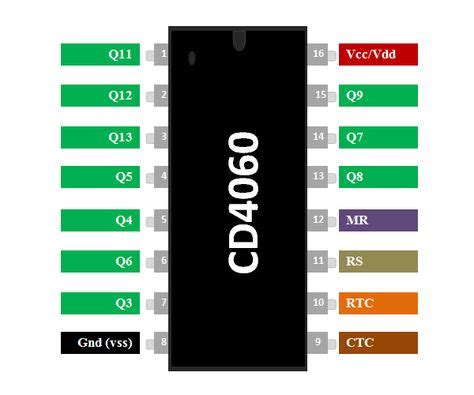
CD4060 Pinout and Pin Functions
The CD4060 pinout and pin functions are as follows:
| Pin | Name | Description |
|---|---|---|
| 1 | Q13 | Counter output 13 |
| 2 | Q12 | Counter output 12 |
| 3 | Q11 | Counter output 11 |
| 4 | Q5 | Counter output 5 |
| 5 | Q4 | Counter output 4 |
| 6 | Q6 | Counter output 6 |
| 7 | Q7 | Counter output 7 |
| 8 | VSS | Ground |
| 9 | Q9 | Counter output 9 |
| 10 | Q8 | Counter output 8 |
| 11 | Q10 | Counter output 10 |
| 12 | Q3 | Counter output 3 |
| 13 | Q2 | Counter output 2 |
| 14 | Q1 | Counter output 1 |
| 15 | RCX | RC oscillator input |
| 16 | VDD | Positive supply voltage |
Oscillator and Reset Pins
- Pin 15 (RCX): This pin is used to connect an external resistor (R) and capacitor (C) to set the oscillator frequency. The oscillator frequency can be calculated using the formula: f = 1 / (2.3 * R * C), where R is in ohms and C is in farads.
- Pin 11 (Q10) and Pin 12 (Q3): These pins can be used for resetting the counter. Connecting either pin to VDD will reset all counter stages to zero.

Internal Architecture and Operation
The CD4060 consists of a 14-stage ripple carry binary counter, an oscillator, and output buffers. The oscillator generates the clock signal for the counter, and its frequency is determined by the external RC network connected to the RCX pin. Each counter stage is a D-type flip-flop that toggles on the falling edge of the clock signal.
The Q outputs of each flip-flop are connected to the corresponding output pins (Q1 to Q13) through 3-state buffers. These buffers allow the outputs to be connected directly to other CMOS circuits or driven by an external signal when the oscillator is gated off.
Frequency Division
The CD4060’s counter stages divide the input oscillator frequency by a factor of 2^n, where n is the stage number. For example, Q1 output has a frequency equal to half the oscillator frequency, Q2 output has a frequency equal to one-fourth the oscillator frequency, and so on. The table below shows the frequency division ratios for each output:
| Output | Division Ratio |
|---|---|
| Q1 | 2 |
| Q2 | 4 |
| Q3 | 8 |
| Q4 | 16 |
| Q5 | 32 |
| Q6 | 64 |
| Q7 | 128 |
| Q8 | 256 |
| Q9 | 512 |
| Q10 | 1024 |
| Q11 | 2048 |
| Q12 | 4096 |
| Q13 | 8192 |

Applications
The CD4060’s versatility makes it suitable for a wide range of applications, including:
-
Frequency Division: The CD4060 can be used to divide a high-frequency signal into lower frequencies for various purposes, such as generating clock signals for microcontrollers or other digital circuits.
-
Time Delay Generation: By using the appropriate output stage, the CD4060 can generate precise time delays ranging from microseconds to several minutes or even hours.
-
Simple Clock Source: The built-in oscillator allows the CD4060 to be used as a standalone clock source for low-frequency applications.
-
Pulse Width Modulation (PWM): By combining the outputs of different stages using logic gates, the CD4060 can generate PWM signals with various duty cycles.
-
Sequencing and Timing: The ripple carry nature of the counter enables the creation of sequencing and timing circuits for control systems, lighting effects, or other timed events.

Circuit Examples
1. Simple LED Flasher
This basic LED Flasher Circuit uses the CD4060’s built-in oscillator and Q5 output to blink an LED at a frequency determined by the R1 and C1 values.
        CD4060
     ___________
    |           |
    |  1     16 |---VDD
    |  2     15 |---[R1]---|
    |  3     14 |          |
    |  4     13 |          |
 LED|--[R2]--12 |          |
    |  6     11 |          |
    |  7     10 |         === C1
    |  8      9 |          |
    |___________|         GND
Components:
– R1: 1 MΩ
– R2: 330 Ω
– C1: 100 nF
– LED: Any standard LED
2. Precision Time Delay Generator
This circuit generates a precise time delay using the CD4060’s Q13 output and an external RC network. The time delay can be adjusted by changing the values of R1 and C1.
        CD4060
     ___________
    |           |
    |  1     16 |---VDD
    |--[R1]--15 |---|
    |  3     14 |    |
    |  4     13 |    |
    |  5     12 |    |
    |  6     11 |    |
    |  7     10 |   === C1
 GND|--8      9 |    |
    |___________|   GND
Components:
– R1: 1 MΩ (adjustable for different time delays)
– C1: 1 µF (adjustable for different time delays)
The time delay can be calculated using the formula: t = 2.3 * R1 * C1 * 8192, where t is in seconds, R1 is in ohms, and C1 is in farads.
Frequently Asked Questions (FAQ)
- What is the maximum oscillator frequency for the CD4060?
-
The maximum oscillator frequency for the CD4060 is typically around 2.5 MHz, depending on the supply voltage and the RC values used.
-
Can the CD4060 be used with a crystal oscillator?
-
While the CD4060 is designed to work with an RC oscillator, it is possible to use a crystal oscillator with some modifications. However, using a dedicated crystal oscillator IC is generally recommended for better stability and reliability.
-
How can I reset the CD4060 counter?
-
The CD4060 counter can be reset by connecting either Q10 (pin 11) or Q3 (pin 12) to the positive supply voltage (VDD). This will reset all counter stages to zero.
-
What is the power supply range for the CD4060?
-
The CD4060 can operate with a wide supply voltage range, typically from 3V to 15V. However, the maximum oscillator frequency and output drive capability may be affected by the supply voltage.
-
Can I cascade multiple CD4060 ICs for longer time delays or lower frequencies?
- Yes, multiple CD4060 ICs can be cascaded by connecting the Q13 output of one IC to the RCX input of the next IC. This allows for even longer time delays or lower frequency outputs.
Conclusion
The CD4060 is a highly versatile and widely used IC that finds applications in various electronic projects, from simple LED flashers to precision timing circuits. Its built-in oscillator, 14-stage ripple carry counter, and 3-state output buffers make it an excellent choice for frequency division, time delay generation, and simple clock sources.
By understanding the CD4060’s pinout, internal architecture, and operating principles, designers can effectively utilize this IC in their projects. The circuit examples provided in this guide serve as a starting point for exploring the CD4060’s capabilities and adapting it to specific application requirements.


Leave a Reply