ALL ABOUT FLEX PCB
-
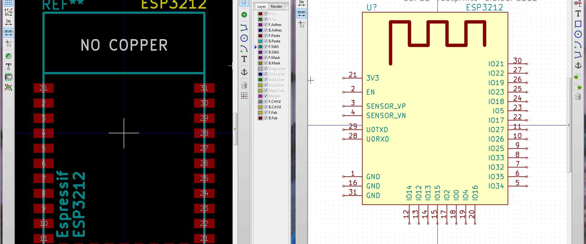
What is a PCB library?
Posted by
–
 Read more: What is a PCB library?
A PCB (printed circuit board) library is a collection of footprint models used in PCB design software to represent real-world components. It contains 3D models and footprint patterns for components like resistors, capacitors, integrated circuits, connectors, etc. PCB libraries allow circuit designers to easily place components on a PCB layout […]
-
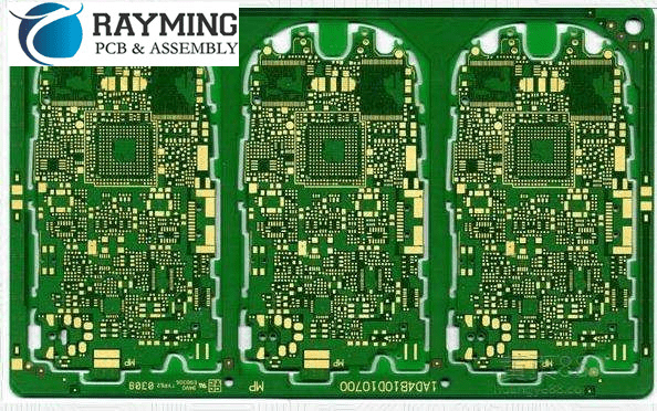
What is PCB milling?
Posted by
–
 Read more: What is PCB milling?
Introduction to PCB milling PCB milling, also known as mechanical milling or routing, is a process used to fabricate printed circuit boards (PCBs). It involves using a computer-controlled milling machine or router to physically remove copper from a substrate to create the traces, pads, and outlines of a PCB design. […]
-
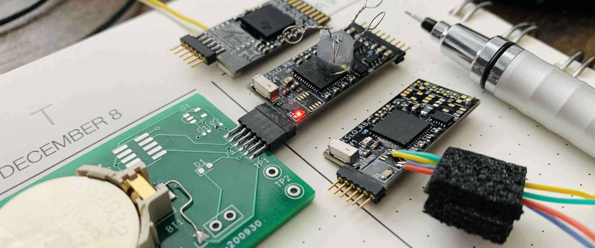
How to Reverse Engineer Printed Circuit Board
Posted by
–
 Read more: How to Reverse Engineer Printed Circuit Board
Introduction Reverse engineering of printed circuit boards (PCBs) involves analyzing an existing board to determine its design, components, and functioning without access to the original schematics or layout files. It is useful for extracting design data from old legacy boards, studying competitors’ products, or debugging equipment issues. While challenging, skilled […]
-
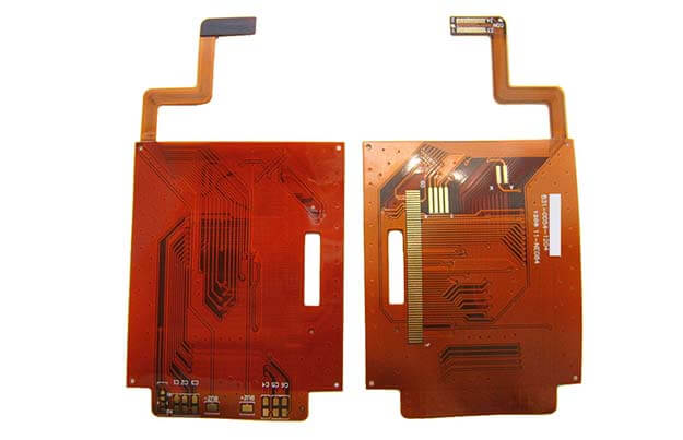
What is Potting a PCB?
Posted by
–
 Read more: What is Potting a PCB?
Introduction Potting is the process of filling the empty spaces on a printed circuit board (PCB) with a protective polymer compound. Potting encapsulates the electronic components and circuitry on the PCB within an insulating material for protection against environmental stresses like moisture, vibration, shock, dust etc. Some key aspects regarding […]
-
What is Quick Turn PCB?
Posted by
–
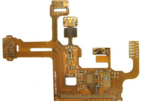 Read more: What is Quick Turn PCB?
Introduction Printed circuit boards (PCBs) are essential components in nearly all modern electronic devices and equipment. They provide the underlying physical structure to mount components and interconnect them into functional circuits. For many electronics projects, getting PCB prototypes produced quickly is crucial for development and testing new designs rapidly. This […]
-
What is a PCB Stackup?
Posted by
–
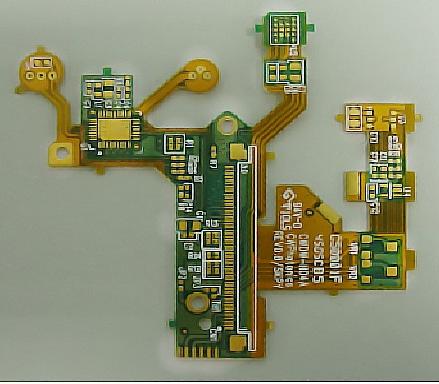 Read more: What is a PCB Stackup?
Introduction to PCB Stackups A printed circuit board (PCB) is made up of multiple layers of conductive and insulating materials laminated together. The sequence of materials that make up the PCB is referred to as the PCB stackup. The stackup defines the layer structure of the PCB and determines its […]
-
What is schematic in PCB?
Posted by
–
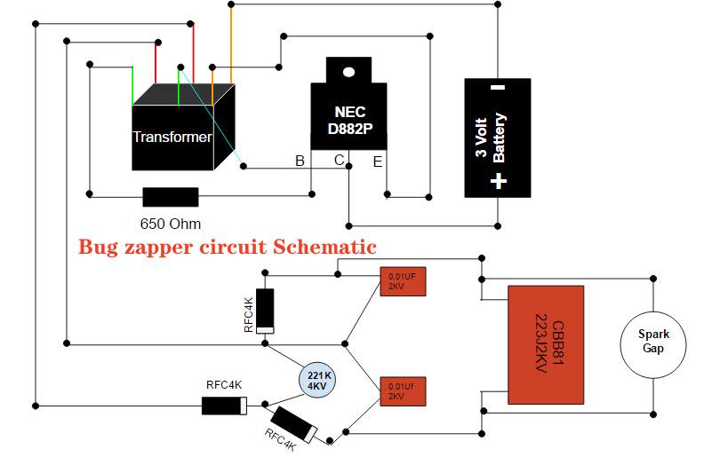 Read more: What is schematic in PCB?
A schematic is a key part of the printed circuit board (PCB) design process. The schematic diagram visually represents the electrical connectivity and functionality of a circuit using standardized symbols and conventions. Developing the schematic is typically the first major step in creating a new PCB design. In this article, […]
-
What is a PCB Stackup?
Posted by
–
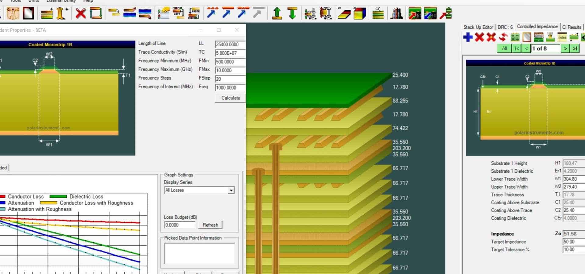 Read more: What is a PCB Stackup?
Introduction A PCB (printed circuit board) stackup refers to the sequence and thickness of conductive copper layers and insulating dielectric materials that make up a multilayer PCB. The stackup defines the structure of the PCB and is a critical factor impacting the performance and manufacturability of the board. Careful stackup […]
-
What is the routing rule for PCB?
Posted by
–
 Read more: What is the routing rule for PCB?
Introduction Printed circuit boards (PCBs) are essential components in electronic devices and equipment. They provide the mechanical support and electrical connections between the various components that make up an electronic circuit. A key aspect of PCB design is routing – determining the paths and channels through which signals travel from […]
-
How to find pcb manufacturers near me
Posted by
–
 Read more: How to find pcb manufacturers near me
Printed circuit boards (PCBs) are essential components in virtually all modern electronic devices. As an electronics designer or engineer, you may need to have PCBs fabricated for prototypes or production runs. Rather than using an overseas PCB manufacturer, you may want to find a PCB production facility close to where […]


