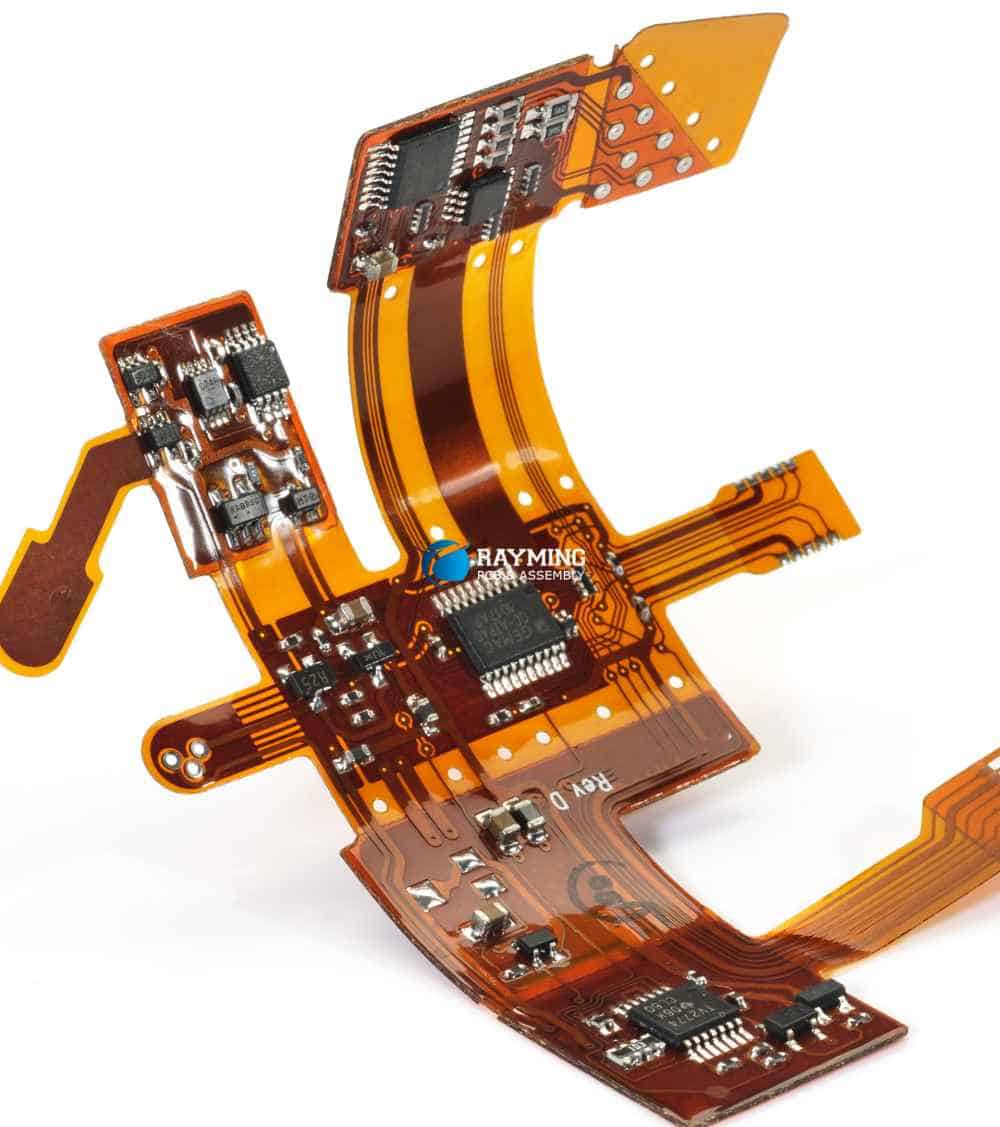
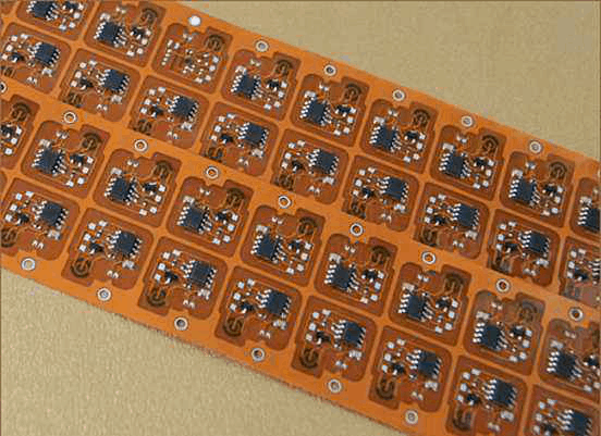
ALL ABOUT FLEX PCB
-
Read more: Who is the manufacturer of PCB assembly in China?
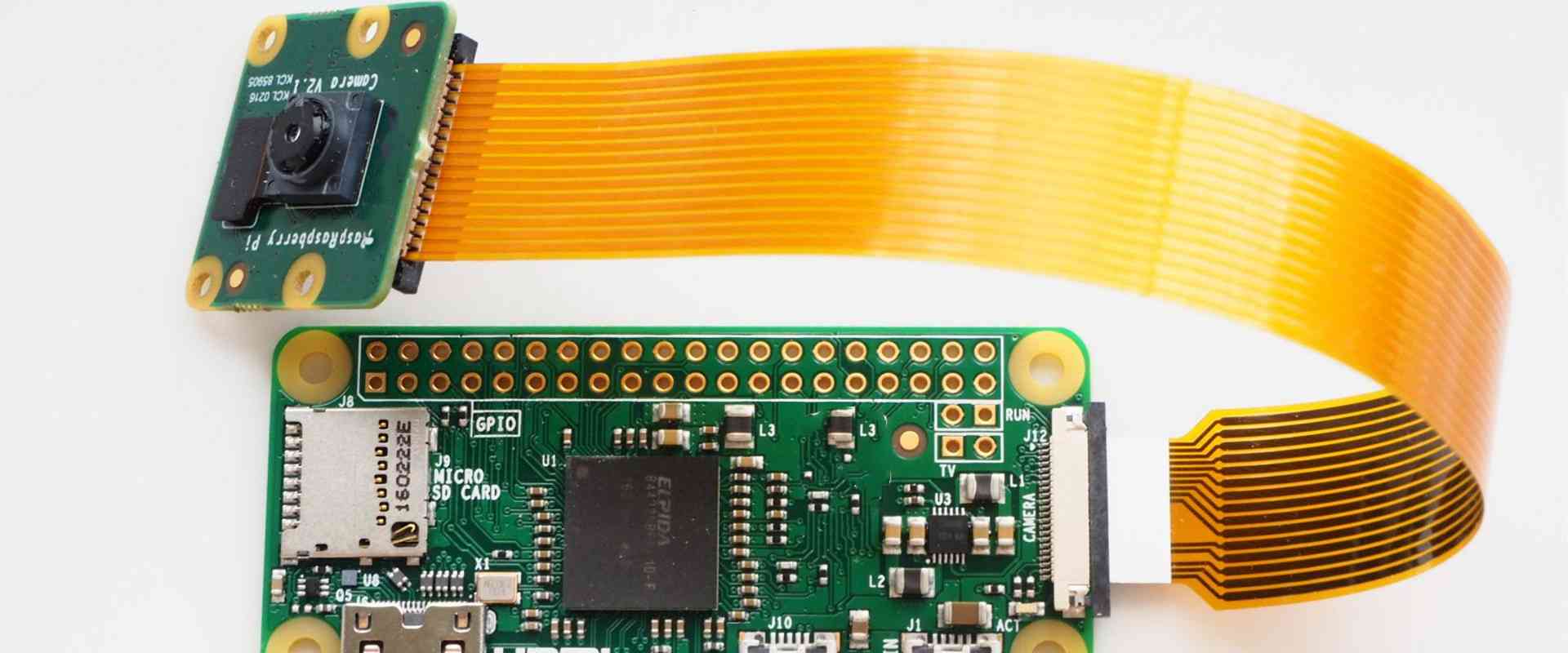
Introduction to PCB Assembly Printed circuit board (PCB) assembly is the process of soldering or assembling electronic components onto a PCB to create a functional electronic circuit. It is an important step in the electronics manufacturing supply chain after the PCB fabrication process. Some key facts about PCB assembly: PCB Assembly Manufacturing in China China…
-
What is a Multilayer PCB?
Posted by
–
 Read more: What is a Multilayer PCB?
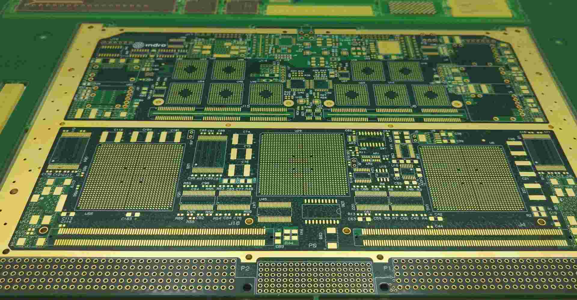
Introduction A multilayer printed circuit board (PCB) is a PCB made up of more than two conductive copper layers separated by dielectric material. Multilayer construction allows greater component density by routing connections between layers using vertical interconnects called vias. This enables more complex circuitry in less space compared to two-layer boards. In a multilayer PCB,…
-
What are aluminum PCBs used for?
Posted by
–
 Read more: What are aluminum PCBs used for?
Introduction to aluminum PCBs Aluminum printed circuit boards (PCBs) are a specialized type of PCB made using aluminum metal as the base substrate instead of the more common FR-4 fiberglass material. Aluminum PCBs were first developed in the 1970s and have seen growing use in recent years for applications requiring high thermal performance, weight savings,…
-
What are the Traces in a PCB?
Posted by
–
 Read more: What are the Traces in a PCB?
A PCB (printed circuit board) mount refers to the method by which a component is mechanically fastened and electrically connected to a PCB. There are several common PCB mount styles, each with their own benefits and drawbacks depending on the application. Some key types of PCB mounts include: Through-Hole Mount Overview Through-hole mounting involves component…
-
What is a PCB Mount?
Posted by
–
 Read more: What is a PCB Mount?
A PCB (printed circuit board) mount refers to the method by which a component is mechanically fastened and electrically connected to a PCB. There are several common PCB mount styles, each with their own benefits and drawbacks depending on the application. Some key types of PCB mounts include: Through-Hole Mount Overview Through-hole mounting involves component…
-
How to DIY PCB at Home?
Posted by
–
 Read more: How to DIY PCB at Home?
Introduction Printed circuit boards (PCBs) serve as the foundation of electronics products, providing the mechanical structure and electrical connections for components. While traditionally made using commercial fabrication, advances in technology now enable DIY PCB prototyping at home. Home PCB fabrication allows rapid design iteration, customization, and cost savings. This guides covers DIY PCB techniques from…
-
What is a PCB Antenna?
Posted by
–
 Read more: What is a PCB Antenna?
Introduction A PCB antenna is an antenna constructed using the same laminate material and manufacturing processes used for printed circuit boards (PCBs). Instead of or in addition to copper traces, the PCB contains carefully shaped copper antenna elements on one or more layers to radiate and receive electromagnetic waves. PCB antennas integrate the antenna directly…
-
What is a PCB stencil?
Posted by
–
 Read more: What is a PCB stencil?
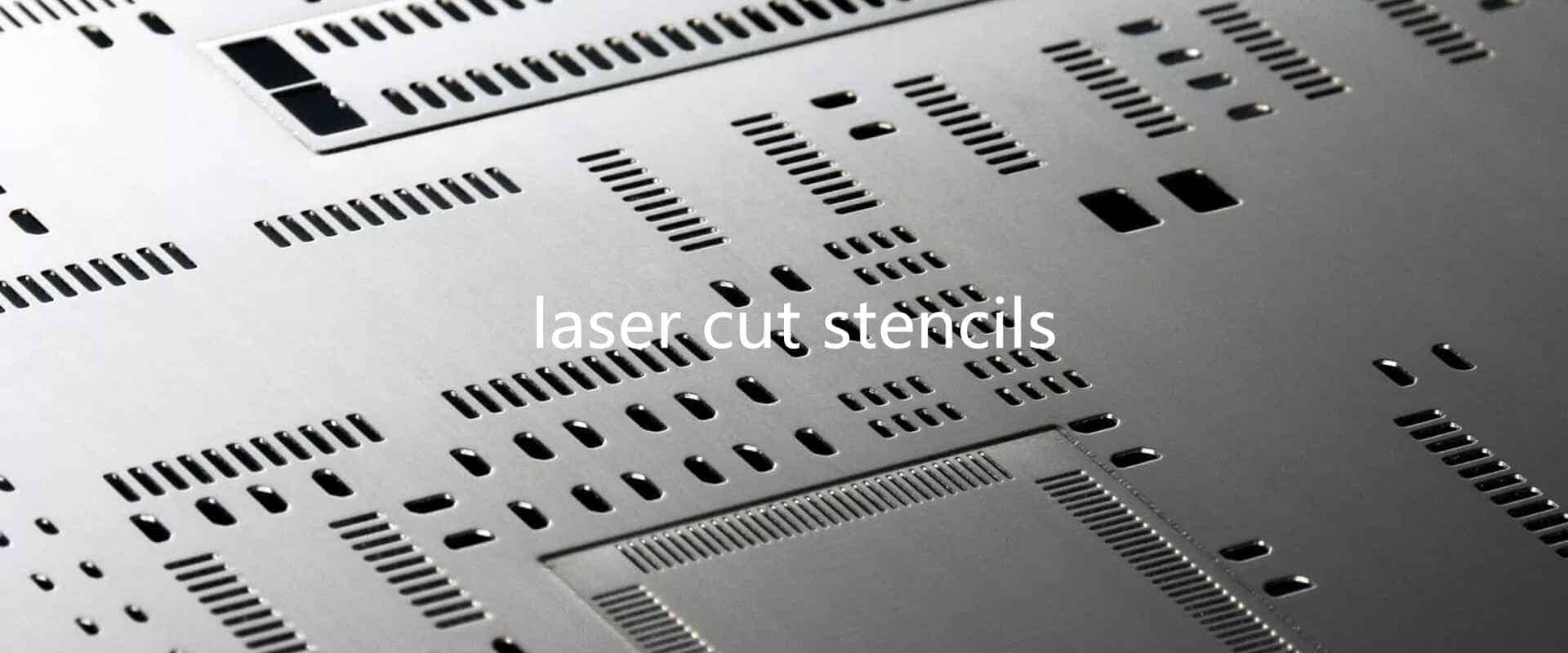
Introduction to PCB stencils A PCB stencil is a thin metal sheet that is used to apply solder paste onto a printed circuit board (PCB) during the surface mount assembly process. The stencil has cutouts that match the pad layout on the PCB, allowing solder paste to be squeezed through onto the pads where components…
-
What is PCB Etching?
Posted by
–
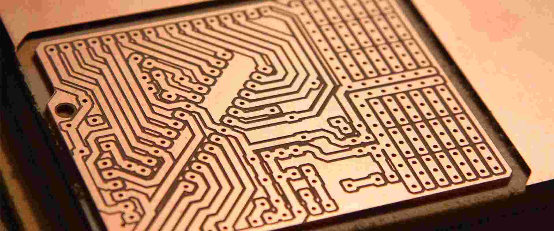 Read more: What is PCB Etching?
Introduction to PCB Etching Printed circuit board (PCB) fabrication involves multiple processes that transform the electrical circuit board design into a physical board. One of the most critical steps is PCB etching. Etching forms the conductive copper traces on the PCB that provide the electrical connections between components. The etching process selectively removes unwanted copper…
-
How to find Online PCB Design?
Posted by
–
 Read more: How to find Online PCB Design?
Introduction Printed circuit boards (PCBs) provide the foundation for electronics products by mechanically supporting and electrically connecting electronic components using conductive pathways or traces. PCB design involves schematic capture, layout, routing, and design verification to transform circuit requirements into a manufacturable board. As PCBs have grown more complex, specialized PCB design software and engineering expertise…


