ALL ABOUT FLEX PCB
-
PCB Stackup Planning Simple
Posted by
–
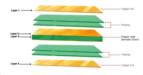
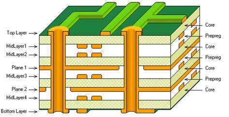
Read more: PCB Stackup Planning SimpleIntroduction to PCB Stackup Printed Circuit Board (PCB) stackup refers to the arrangement of copper layers and insulating materials that make up a PCB. Proper PCB stackup planning is crucial for ensuring the optimal performance, reliability, and manufacturability of electronic devices. In this comprehensive guide, we will delve into the […]
-
PCB Grounding Techniques
Posted by
–
 Read more: PCB Grounding Techniques
Introduction to PCB Grounding Printed Circuit Board (PCB) grounding is a critical aspect of electronic design that ensures the proper functioning, reliability, and stability of electronic circuits. Grounding techniques involve creating a low-impedance path for electrical currents to return to their source, minimizing noise, and preventing interference between different parts […]
-
PCB design with copper foil thickness traces the relationship between the width and currents
Posted by
–
 Read more: PCB design with copper foil thickness traces the relationship between the width and currents
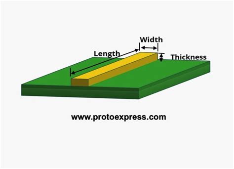
Introduction to PCB Copper Trace Width and Current Printed circuit boards (PCBs) are the foundation of nearly all modern electronics. Proper PCB design is critical to ensure reliable operation, signal integrity, power delivery, and heat dissipation. One of the most important aspects of PCB design is selecting the appropriate width […]
-
 Read more: Using Return Paths that Follow Least Impedance to create a better PCB Design
What are Return Paths in PCB Design? In PCB design, a return path is the path that electric current takes to return to its source, completing the circuit. Every signal trace on a PCB has an associated return path. At low frequencies, the return path follows the path of least […]
-
RAYPCB -standard-stackup-for-multilayer-pcbs
Posted by
–
 Read more: RAYPCB -standard-stackup-for-multilayer-pcbs
What is a PCB Stackup? A printed circuit board (PCB) stackup refers to the arrangement of copper and insulating layers that make up a PCB. The stackup defines the number of layers, the thickness of each layer, the materials used, and the interconnections between layers. The stackup is a critical […]
-
Advanced Circuits Terms and Conditions
Posted by
–
 Read more: Advanced Circuits Terms and Conditions
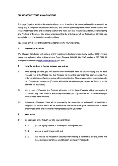
Overview of Terms and Conditions Advanced Circuits provides printed circuit board (PCB) fabrication and assembly services to customers worldwide. By placing an order with Advanced Circuits, customers agree to abide by the company’s terms and conditions. These terms cover key aspects of the business relationship between Advanced Circuits and its […]
-
 Read more: 6 Proven Working Tips to Find Good SMT Manufacturers
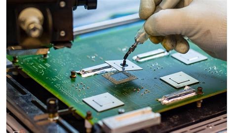
1. Research and Identify Potential SMT Manufacturers The first step in finding a good SMT manufacturer is to conduct thorough research and identify potential candidates. Here are some ways to do this: 1.1 Online Directories and Industry Associations Utilize online directories and industry associations to find SMT manufacturers. Some popular […]
-
 Read more: PCB Layout Techniques to Achieve RF Immunity for Audio Amplifiers
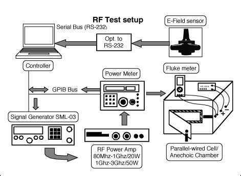
Understanding RF Interference and Coupling Mechanisms Radio frequency interference (RFI) refers to unwanted high frequency signals that can disrupt normal circuit operation. As the number of RF emitting devices like smartphones, Bluetooth accessories, and IoT devices continues to proliferate, RFI is an increasing concern for audio designers. There are several […]
-
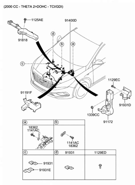 Read more: Beijing Hyundai Sang Nata central locking circuit diagram
Introduction to Hyundai Sonata wiring diagram The Hyundai Sonata is a popular mid-size sedan known for its reliability, comfort, and affordability. As with any vehicle, understanding the wiring diagram is essential for proper maintenance, troubleshooting, and repairs. In this article, we will focus on the central locking circuit diagram of […]
-
Fly Buck converter PCB layout tips
Posted by
–
 Read more: Fly Buck converter PCB layout tips
Introduction to Fly Buck Converters and PCB layout Fly buck converters, also known as isolated buck converters, are widely used in power electronics to step down high voltages to lower levels while providing electrical isolation between the input and output. These converters play a crucial role in various applications, including […]


