ALL ABOUT FLEX PCB
-
Read more: ESP32 Projects: Low Power, Low-Cost Integrated Circuit Projects
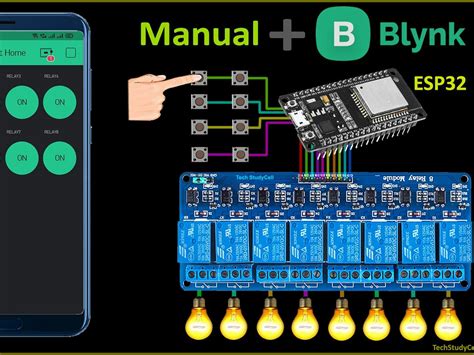
Introduction to ESP32 The ESP32 is a low-cost, low-power system on a chip (SoC) series with Wi-Fi & dual-mode Bluetooth capabilities. It is designed and developed by Espressif Systems, a Shanghai-based Chinese company. The ESP32 series employs a Tensilica Xtensa LX6 microprocessor in both dual-core and single-core variations and includes […]
-
 Read more: Ball Grid Array: A Dense Surface Mount Package for Integrated Circuits
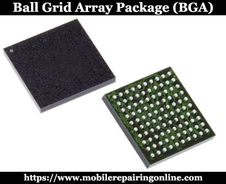
What is a Ball Grid Array (BGA)? A Ball Grid Array (BGA) is a type of surface-mount packaging used for integrated circuits (ICs). It utilizes a grid of solder balls on the bottom side of the package to provide electrical connections between the IC and the printed circuit board (PCB). […]
-
 Read more: How to Determine if Your Product is HDI or A Regular PCB Board
What is a Regular PCB? A regular PCB, also known as a conventional PCB, is a printed circuit board that consists of conductive tracks, pads, and other features etched from copper sheets laminated onto a non-conductive substrate. These boards are used to mechanically support and electrically connect electronic components using […]
-
Back Drill PCB: What It Is and How to Use It
Posted by
–
 Read more: Back Drill PCB: What It Is and How to Use It
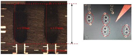
What is PCB Back Drilling? PCB back drilling, also known as controlled depth drilling or back-drill, is a process used in the manufacturing of high-speed printed circuit boards (PCBs) to remove the unused portion of a plated through-hole (PTH) that extends beyond the last layer of the PCB. This technique […]
-
 Read more: Top 17 Electronics Manufacture Trade Show for 2023 – 2024
1. CES (Consumer Electronics Show) Date: January 5-8, 2023 | January 9-12, 2024 Location: Las Vegas, Nevada, USA Website: https://www.ces.tech/ CES is the world’s largest and most influential technology event, showcasing the latest innovations in consumer electronics, including smartphones, wearables, smart home devices, and more. With over 4,500 exhibitors and […]
-
4×4 keypad: An In-depth Guide
Posted by
–
 Read more: 4×4 keypad: An In-depth Guide
Introduction to 4×4 Keypads A 4×4 keypad is a matrix-style input device commonly used in electronic projects, such as microcontroller-based systems, to provide a user-friendly interface for data entry. The keypad consists of 16 buttons arranged in a 4×4 grid, allowing users to input numbers, letters, and symbols. This comprehensive […]
-
 Read more: HDI PCB Design-Create the Most Suitable for Your Needs
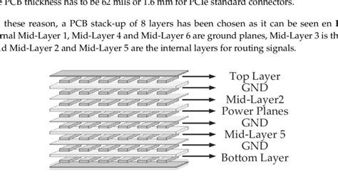
Introduction to HDI PCBs High Density Interconnect (HDI) Printed Circuit Boards (PCBs) are a type of circuit board that offers higher wiring density than traditional PCBs. HDI PCBs have finer lines and spaces (<100 μm), smaller vias (<150 μm), and capture pads (<400 μm), and higher connection pad density (>20 […]
-
PCB Fabrication—What You Need To Know About
Posted by
–
 Read more: PCB Fabrication—What You Need To Know About
Introduction to PCB Fabrication Printed Circuit Board (PCB) fabrication is the process of creating printed circuit boards used in electronic devices. PCBs provide the physical structure and electrical connections for components like resistors, capacitors, and integrated circuits. The PCB fabrication process turns a design into a functional board ready for […]
-
Printed circuit board materials
Posted by
–
 Read more: Printed circuit board materials
Introduction to PCB materials Printed Circuit Boards (PCBs) are the backbone of modern electronics, providing a reliable and efficient means of connecting electronic components. The choice of materials used in PCB Fabrication plays a crucial role in determining the performance, durability, and cost of the final product. In this comprehensive […]
-
Conductive vs. Non-Conductive Via Fill PCB
Posted by
–
 Read more: Conductive vs. Non-Conductive Via Fill PCB
Introduction to Via Fill in PCB Design In the world of printed circuit board (PCB) design, vias play a crucial role in connecting different layers of the board. Vias are essentially small holes drilled through the PCB that allow electrical connections to be made between different layers. There are two […]


